
SMART Photonics PDK supporting export to multiple layout tools
VPIphotonics has announced the release of an updated VPItoolkit supporting the SMART Photonics Process Design Kit (PDK), which seamlessly integrates Photonic Integrated Circuit (PIC) simulation and automated mask layout extraction.
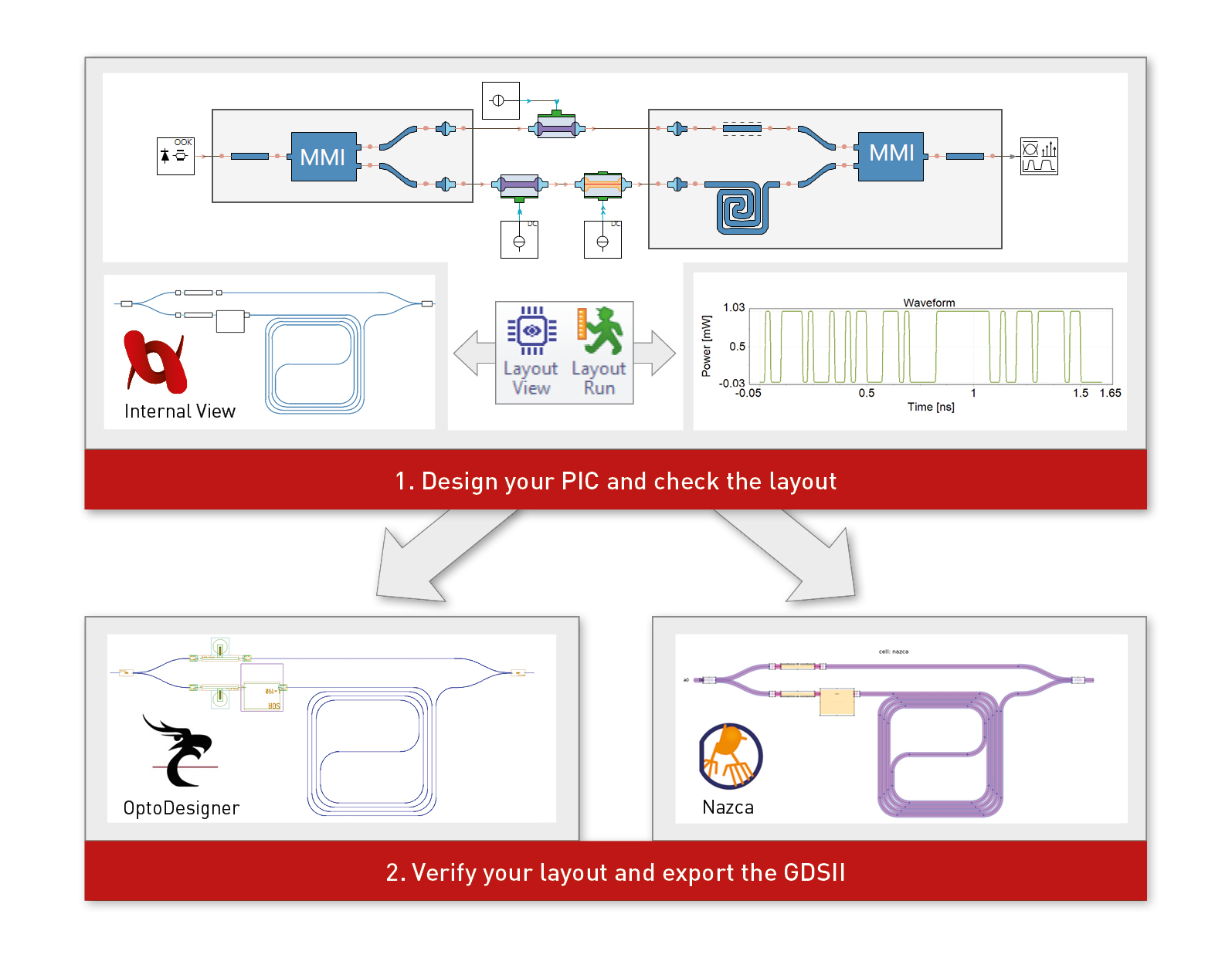
The free and open-source Nazca Design framework is now fully supported for the generation of verified PICs layouts to be submitted and processed in terms of Multi-Project Wafer (MPW) runs on SMART Photonics' Indium Phosphide technology platform. Nazca Design supports commercial PDKs and IP-blocks and is created and supported by BRIGHT Photonics, a design house dedicated to improve PIC design through open innovation. Similar mask export capabilities with OptoDesigner developed by PhoeniX Software (part of Synopsys) have already been introduced earlier.
VPItoolkit PDK SMART v1.4 constitutes a library extension to VPIcomponentMaker Photonic Circuits "“ the professional simulation and design environment for large-scale PICs with a mix of photonic, electrical and optoelectronic devices. The new toolkit version broadens the selection of available building blocks with designer-defined models and layouts, making a step toward functional photonic design automation.
With the new SMART PDK toolkit, designers are able to construct their own custom building blocks, effectively expanding the foundry PDK to fit individual needs. Custom compact models and layout geometry are defined via Python-enabled scripting and paired in VPIcomponentMaker Photonic Circuits, where they are simulated together with a broad set of available standard building blocks of the SMART PDK and flexible connectors.
By employing parameterized designs, users can investigate a large number of PIC variations and generate the associated layouts in a matter of a few clicks. Sweeping and optimization of layout parameters are conveniently supported, together with a large set of instrumentation tools for automated data analysis.
With the use of the new VPI-internal Layout View, designers can quickly visualize and proof their work for eminent mistakes and geometry inconsistencies without the need of external applications. Once a satisfactory PIC implementation has been obtained, the mask layout can be extracted and further processed using the preferred layout tool, without requiring any change in the simulation setup. After the layout is checked for foundry design rules, a verified GDSII file is generated for submission to SMART Photonics for fabrication.
These new capabilities are shown for the first time at ECOC, Sep 24-26 2018 in Rome "“ visit the VPIphotonics team at booth 302 for a live demonstration.


