JePPIX Training in Eindhoven 2018
The JePPIX deep-dive technology training is scheduled for two weeks starting from Monday 29th October 2018. The registration is now open. The course covers the theory and practice of integrated photonic component and circuit design using the powerful JePPIX building blocks. Hands on training with lab tools and design tools are complemented with clean room tours to develop insights into design rules. Layout and simulation methods are developed with JePPIX CAD tool developers and professional designers. This course is particularly suitable to engineers who wish to create their first MPW chips.
In the first week, trainees will develop insights into mode analysis to better understand the design space for waveguide based integrated optics, how best to construct interferometers and filters. Active building blocks including semiconductor optical amplifiers, modulators and detectors will be introduced in terms of physical principles and practical implementation as components and circuit elements. Methods for laying out circuits will be developed. Hybrid and monolithic integration schemes will be described.
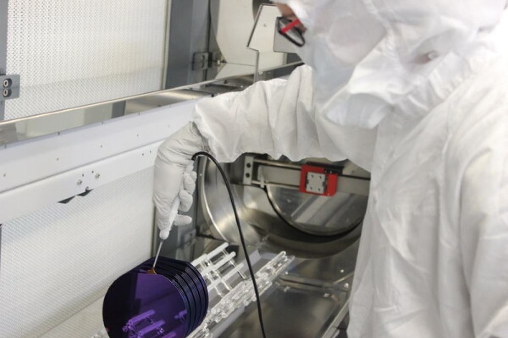
In the second week, the emphasis turns to practical skills, with the opportunity to trial commercial CAD tools, process design kits (PDKs) and develop insights with expert designers and leading academic instructors. Representatives from the foundries will also be available to talk through the latest platform capabilities. Visits to clean room facilities and measurements laboratories are included to provide insights into the role of fabrication tolerances and testing methods on design methods. Packaging will also be reviewed to ensure package, test and manufacture aware design.
The course is expected to be relevant to engineers and scientists who have an awareness of photonics and the underlying principles, and who wish to extend this knowledge to create the first photonic integrated circuits on open access foundries. The course will provide both the underlying knowhow to enable an understanding of the design space, as well as the practical skills to implement designs. Participants with specific circuit specifications in mind may also benefit by being able to think through their designs with on-site experts.
Learning outcomes are expected to include the ability to identify and specify building blocks, connect building blocks and lay out for the creation of functional photonic integrated circuits. Participants will use a range of simulation and design tools suited for active and passive components and circuits, and be able to use foundry specific process design kits to predict circuit performance and create the file sets required for an MPW (multi-project wafer) run.
http://www.jeppix.eu/training2018/


