ePIXfab organise summer school and design course
After two successful editions with participants from across the globe, ePIXfab organizes the 3rd edition of its Silicon Photonics Summer School. We combine this back-to-back with the second edition of the focused Specialist Course on Silicon Photonics Design.
The summer school runs from 11th to 15th June 2018 and is followed by the design course from 18th to 22nd June 2018 at Ghent University (Belgium). The two modules can be taken together or separately.
Summer School: Target Audience & Scope
The Silicon Photonics Summer School is designed to equally benefit the beginners and experts in the field of silicon photonics. It will expose the participants to the fundamental concepts of silicon photonics. Also, it will provide the participants with a unique opportunity to get a strong insight into the latest developments in the field, and give insight in the many application fields where silicon photonic is, or will be, making an impact. Renowned speakers in the field of silicon photonics will showcase hot topics and latest research results for various applications of silicon photonics. The summer school has two poster sessions at the summer school. The goal of the poster session is to provide the participants with an opportunity to interact with world-renowned experts of silicon photonics to discuss their ideas and potential challenges.
Design Course: Target Audience & Scope
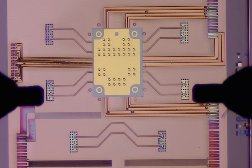
The Specialist Course on Silicon Photonics Design offers a focused, hands-on design course. It is targeted at researchers and engineers with an already fundamental understanding of photonic integrated circuits. The course focused on the process to translate a photonic circuit idea into a working chip, going from schematic design and circuit simulation to layout, routing and interactive design rule checking. As part of the course, the participants get the opportunity to actually tape-out a design that will be fabricated with an e-beam prototyping service and characterized. Based on these results, the design can be improved and submitted to a wafer-scale multi-project-wafer run of which the participants will receive the final chips.


