NSF awards $1.2 million to leverage AIM Photonics' R&D and foundry capabilities

The American Institute for Manufacturing Integrated Photonics (AIM Photonics), a Department of Defence-led public-private partnership headquartered in New York State to advance the nation's photonics manufacturing capabilities, today announced that three National Science Foundation (NSF) funded grants totalling $1.2 million will enable collaborative photonics-centred R&D with the Rochester Institute of Technology (RIT), University of California-San Diego (UCSD), and University of Delaware (UD), respectively.
"AIM Photonics is thrilled to work with leading academic institutions including RIT, UCSD, and UD on these three separate, NSF-funded projects to collaboratively enable photonics-focused devices and capabilities that can allow for the more efficient identification of materials, as well as enhanced processes for manufacturing complex photonic devices and next-generation computing capabilities. We are proud to be the central driver of photonics-based advances that can significantly improve the technologies our society depends on," said Dr. Michael Liehr, CEO of AIM Photonics.
"Partnering with AIM Photonics provides NSF-funded researchers unique access to world-class manufacturing facilities, stimulating innovation and enabling faculty to span the spectrum from fundamental research breakthroughs to translational advances in integrated photonics devices and circuits that directly impact society," said Dr. Filbert Bartoli, Director of the Division of Electrical, Communications and Cyber Systems in NSF's Directorate for Engineering.
Rochester Institute of Technology "“ AIM Photonics Project
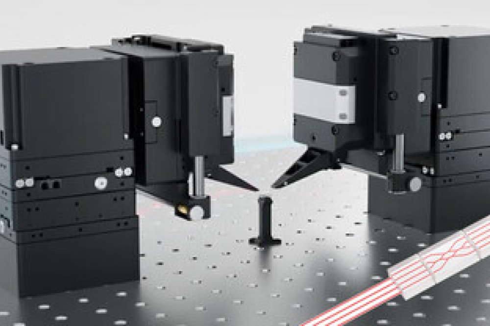
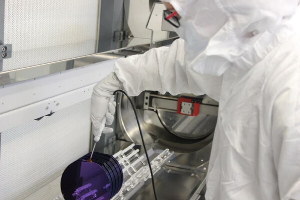
The NSF awarded RIT $423,000 as part of the research project, "PIC: Hybrid Silicon Electronic-Photonic Integrated Neuromorphic Networks," which will focus on realizing high-performance neural networks that will be integrated onto photonic chips for scalable and efficient architectures that, in tandem with integrated electronics, overcome challenges related to photonic memory and amplification"”offering a hybrid, high-bandwidth computing approach for applications to autonomous systems, information networks, cybersecurity, and robotics. To develop these architectures, RIT will work with AIM Photonics to use its leading-edge PIC toolset, located at SUNY Polytechnic Institute in Albany, NY, and the AIM Photonics TAP facility in Rochester, NY"”the world's first 300mm open access PIC Test, Assembly, and Packaging (TAP) facility. The project will take place within RIT's Future Photon Initiative (FPI) and Center for Human-Aware AI (CHAI).
This research effort will also provide educational opportunities for elementary through high school, undergraduate, and graduate students, and the AIM Photonics Academy will be able to disseminate the project's findings to further increase understanding of this fast-growing area of research.
"We are excited to partner with AIM Photonics on this research project. The hybrid electronic-photonic neuromorphic chips my Co-PI (Professor Dhireesha Kudithipudi) and I are developing are directly enabled by the state-of-the-art PIC and TAP capabilities of AIM Photonics," said Project Principal Investigator, Professor Stefan Preble at Rochester Institute of Technology's Kate Gleason College of Engineering.
University of California-San Diego "“ AIM Photonics Project
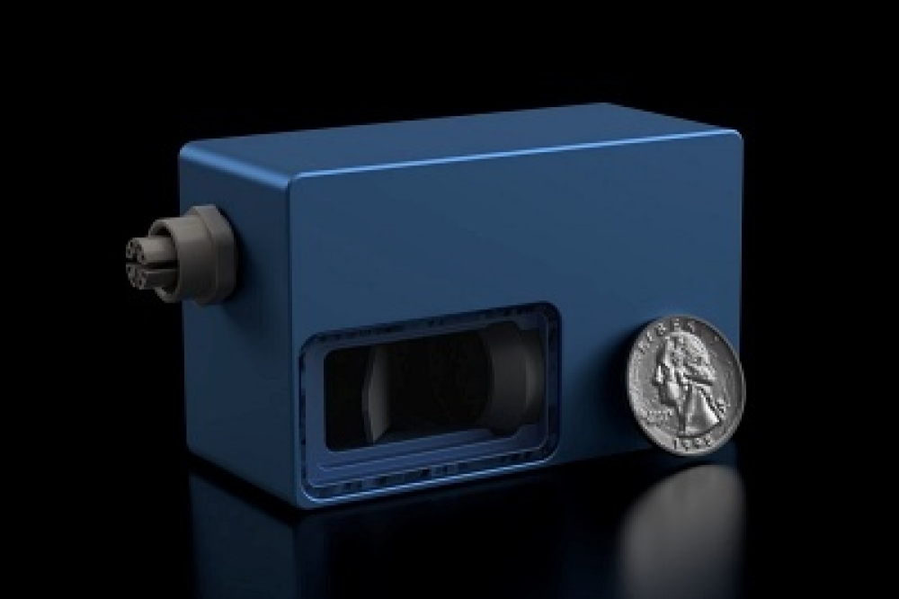
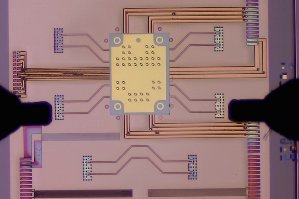
The NSF awarded UCSD $405,000 for research entitled, "PIC: Mobile in Situ Fourier Transform Spectrometer on a Chip," which will enable UCSD to rapidly prototype and test miniaturized and mobile platform-embedded optical spectrometers that will excel at chemical identification. The initial design, fabrication, and validation of such a spectrometer on a Si chip have been recently reported in Nature Communications 9:665 (2018). This effort will continue and culminate with full-scale manufacturing runs at AIM Photonics' foundry at the Albany Nanotech Complex. The integrated chip-scale Fourier transform spectrometer is to be fully CMOS compatible for use in mobile phones and other mobile platforms with potential impacts in areas ranging from environmental management, medicine, and security.
Undergraduate and graduate students at the institution will also be able to gain hands-on training as the research project simultaneously serves as a community outreach tool to inspire students attending middle and high schools.
"Moreover, we are also developing an educational silicon photonics kit through the NSF's ERC-CIAN (Engineering Research Center for Integrated Access Networks) and in collaboration with Tyndall National Institute at University College Cork (Ireland). The kit will initially be implemented in an undergraduate lab curriculum with the goal to prepare the future task force through hands-on experience in this evolving field," said Project Principal Investigator, Professor Yeshaiahu Fainman, Cymer Chair in Advanced Optical Technologies and Distinguished Professor at the University of California-San Diego.
University of Delaware "“ AIM Photonics Project
The NSF awarded UD $360,000 as part of the research project, "PIC: Hybrid Integration of Electro-Optic and Semiconductor Photonic Devices and Circuits with the AIM Photonics Institute." This effort will allow UD to work with AIM Photonics to leverage the initiative's expertise and state-of-the-art foundry for the development of new heterogeneous manufacturing processes for photonic devices, using new materials such as Lithium Niobate (LiNbO3), which can then be directly integrated with silicon CMOS systems for photonic devices and chip scale systems.
More specifically, the effort aims to realize high performance RF-photonic devices such as ultra-high frequency modulators (> 100 GHz) that are used in data networks; high-efficiency chip-scale routers for advanced data centers; and high-power phased array antenna photonic feed networks that are compatible with older and next-generation wireless communications; in addition to enabling a number of other wide-ranging commercial applications.
"The heterogeneous integration of LiNbO3 with Silicon Photonics allows for the use of the best properties of both material systems, thereby enabling truly innovative systems for countless emerging applications," said Project Principal Investigator, Dr. Dennis Prather, Engineering Alumni Professor at the University of Delaware.
AIM Photonics features research, development, and commercialization nodes in Albany, NY, at SUNY Polytechnic Institute, as well as in Rochester, NY, where state-of-the-art equipment and tools are being installed at AIM Photonics' TAP facility. The initiative also includes an outreach and referral network with the University of Rochester, Rochester Institute for Technology, Columbia University, Massachusetts Institute of Technology, University of California - Santa Barbara, University of Arizona, as well as New York State community colleges. In total AIM Photonics includes more than 100 signed members, partners, and additional interested collaborators.


