Thinking beyond conventional silicon photonics

Photonic integrated circuits (PICs) owes its birth to III-V compound semiconductors, and the traditional field of optoelectronics that has been built around these versatile materials since the 1960s. Since the 1980s, though, silicon photonics has slowly but surely been pursued as an alternative platform. Realized primarily through silicon-on-insulator (SOI) wafers, the argued advantages of silicon over III-V PICs have been much more compact optical waveguides with lower optical propagation loss, better processing yield, lower cost and compatibility with silicon foundry processing. Integration with CMOS electronics is another advantage, historically, but it is much less critical these days, as the trend is to have photonics and electronics on separate chips. Nonetheless, it was clear from the get-go that there is no "pure silicon" photonics, since other materials are inevitably required for a variety of functionalities that cannot be easily achieved in silicon. Some of the widely known shortcomings of silicon for integrated photonics are: (a) Lack of light generation [due to silicon's indirect bandgap]; (b) Negligible photodetection in the telecom range and above [due to silicon's bandgap energy]; (c) Lack of electrooptic or Pockels effect and second-order optical nonlinearity [due to silicon's centrosymmetric crystal symmetry]; (d) Inefficient third-order optical nonlinearity below 2.2 μm [due to nonlinear absorptions]; (e) Loss of the buried oxide (BOX) layer of SOI in the mid-infrared wavelengths [1].
Addressing the former two shortcomings was more critical in the development of the silicon photonics technology for its prime application: datacom. Integrating thin layers of germanium in waveguide photodetector configuration has long been a standard procedure, hence group-IV photonics has been a common term for the technology too. Meanwhile, despite tremendous amount of efforts, dependable silicon-based lasers remain elusive to date. Instead and despite certain downsides, various methods for hybrid integration of III-V lasers have been successfully developed and are widely in use in commercial transceiver chips. Given this, maybe "groups III-to-V photonics" is semantically a more accurate descriptive name for silicon photonics.
The mentioned lack of "˜true' electrooptic effect in silicon has been circumvented by the less attractive phenomenon of plasma dispersion effect, in which the free-carrier density is modulated electronically, usually via a p-n junction diode straddling SOI waveguides. Reasonably high data transmission rates are routinely achieved, but silicon modulators inherently suffer from low extinction ratios or modulation depths, limited to a few dB, particularly at the high data rates of interest. Such low performance may be acceptable for current datacom applications, where fiber-optic links with on-off keying reaching to a maximum of a couple kilometers are targeted. However, if it is intended to expand the realm of silicon photonics to longer links and/or more advanced modulation formats, the low extinction ratio of modulators based on plasma dispersion effect will become a bottleneck for system performance.
The best-known phenomenon and material for optical modulation is the electrooptic or Pockels effect in lithium niobate. Dominating the long-haul communication market for decades, lithium niobate Mach-Zehnder modulators boast low loss, remarkably high modulation depths of higher than 20 dB and modulation bandwidths of up to 100 GHz. The challenge for this technology is that the devices are bulky, power-hungry, expensive and do not lend themselves easily for integration of multiple devices. The root problem is the common waveguide formation techniques of proton exchange or titanium indiffusion, resulting in low-index-contrast waveguides and, in turn, leading to large drive voltages, length and bending radii. Therefore, a high-contrast and low-loss lithium niobate waveguide technology is desirable. In addition, if the lithium niobate photonics technology is merged with silicon photonics at the back end of line (BEOL) portion of foundry fabrication, it could be game-changing.
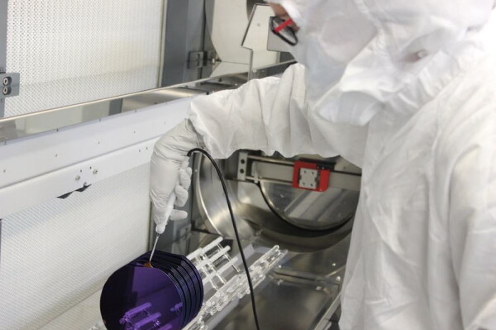
To this end, the author's group at CREOL has been working on developing such a technology for several years. We reported the first lithium niobate on silicon wafers, waveguides and modulators in 2013 [2]. The in-house fabrication process actually resembles the SmartCut method of SOI and involves ion implantation of bulk lithium niobate wafers, bonded to oxidized silicon wafers, followed by thermal slicing to leave a thin film (200 to 600 nm) of lithium niobate on a silicon dioxide insulating layer, serving as the bottom cladding of the waveguides.
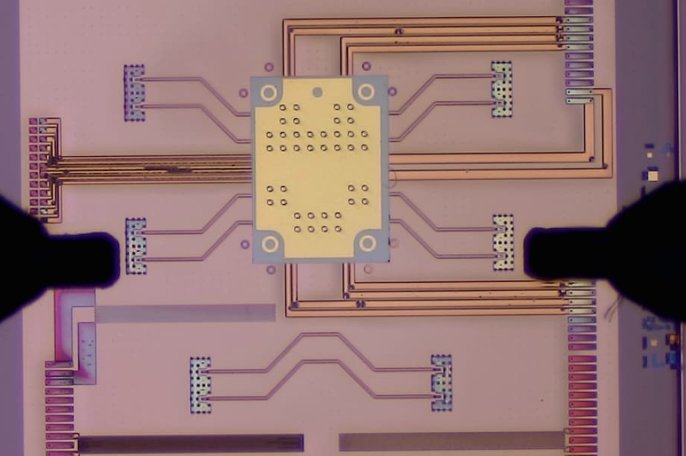
In principle, dry etching of lithium niobate can be used for ridge formation and lateral optical confinement. In practice and to avoid the challenges of etching lithium niobate, we have been typically relying on the simpler and more reliable solution of rib-loading the thin films. The choice of the rib material is not that critical, as long as its refractive index roughly matches that of lithium niobate, can provide low loss and it is easy to process. Based on this maturing waveguide platform and in a series of research papers [2-4], we have so far successfully reported the first lithium niobate microring and Mach-Zehnder modulators on silicon. The latest generation of Mach-Zehnder modulators possess a 3-dB bandwidth of 33 GHz, low half-wave voltage length product of 3.1 V.cm at DC and less than 6.5 V.cm up to 50 GHz. Notable is the high extinction ratio of 18 to 20 dB in the devices, on par with commercial lithium niobate devices and much higher than the mentioned plasma dispersion effect in silicon. Optimized designs confirm that devices with up to 100 GHz bandwidth are attainable.
Encouraged by the above promising results, our research team has established a spin-off company, Partow Technologies (http://www.partow-tech.com/). The company has already been marketing the lithium niobate on silicon wafers for three years for photonic and non-photonic applications and is progressing towards commercializing thin-film modulators and other photonic circuits on the heterogeneous wafers.
The previously mentioned issues pertaining to light generation, detection and modulation are not the only shortcomings of silicon photonics. For example, other issues arise for nonlinear and mid-infrared applications. Although these applications may not have a large market yet or the solutions may not be ready for commercialization, they may become important in future developments.
Lack of electrooptic or Pockels effect in silicon is tightly related to the lack of second-order optical nonlinearity. The associated nonlinear phenomena have potential applications in light sources at lower (e.g., via second-harmonic generation) or higher (e.g., via difference-frequency generation) wavelengths than a pump source's, self-referencing in optical combs, quantum photonics at telecom wavelengths, and more. Readily, the discussed lithium niobate platform can be exploited for such nonlinear frequency conversion applications. We have accordingly reported second-harmonic generation and entangled photon generation. Typically, phase-matching techniques are required for efficient conversion. We have applied the conventional period poling, as well as a novel method, dubbed mode-shape modulation, to address this requirement [5, 6].
Third-order optical nonlinearities also have a whole host of applications, for example four-wave mixing and continuum generation. Silicon has high third-order nonlinearity but at wavelengths below the two-photon bandgap of ~ 2.2 μm, the Kerr and Raman nonlinear effects are significantly hampered by nonlinear absorptions. Although carrier sweep-out techniques alleviate the issue to a certain extent, for the most part researchers have moved to other highly nonlinear materials such as silicon nitride and chalcogenide glass to form waveguides for nonlinear applications on silicon [1, 7].
An emerging research area is the quest for simultaneously integrating all these materials on the same chips. For example, it is key to "co-integrate" cascaded waveguides with second- and third-order nonlinearities for frequency-stabilized optical comb generation. Chalcogenide or silicon nitride waveguides can be exploited to achieve octave-spanning supercontinuum generation (SCG), while second-harmonic generation in lithium niobate can be used for stabilization by f-to-2f carrier-envelope offset (CEO) locking. We have recently reported progress towards such multimaterial integration, in which light enters a top-layer chalcogenide waveguide and then it is directed by adiabatic tapers into a lithium niobate underneath waveguide [8].
Last but not least, mid-infrared wavelengths (~ 3 to 5 μm) could be another up-and-coming application of silicon photonics. The challenge here is that the BOX bottom clad layer of the standard SOI waveguides is lossy at certain bands within this wavelength range. In order to eliminate oxide from silicon waveguide structures, our team reported the first silicon-on-nitride waveguides in 2013 [9]. We later reported two types of all-silicon air-clad suspended- and anchored-membrane waveguides [10, 11], which do not rely on wet etching the BOX layer. Rather, mechanically robust mid-infrared waveguides are achieved by trench formation in bulk silicon, bonded to an SOI die followed by substrate removal.
Given the limited space, the above focuses on the works demonstrated in the author's lab. But they are just examples of a trend in moving away from the standard silicon photonics technology based on SOI waveguides/III-V lasers/germanium detectors. Many other teams around the globe are working on similar or other platforms, all aimed at increasing the performance of existing functionalities or at adding new functionalities. The common theme of all of them is heterogeneous integration of multiple materials for various devices and circuit segments on the same chip, preferably on silicon substrates. It is interesting that the alternative to such heterogeneous approaches is perhaps nothing but III-V PICs, provided that their mentioned issues of compactness, low loss, processing yield and cost are solved.


