Leti's high performance computing design utilizes robust WDM optical links on photonic interposers

In the past years, silicon photonics technology has matured to the point that it can be used in commercial products. For instance, photonic transceivers now connect racks optically in data centers, with data rates from 100 Gbps and beyond. Such products are delivered by several companies, such as Intel, Mellanox, Luxtera, and so on, and will shortly reach 400 Gbps using WDM (Wavelength Division Multiplexing) techniques and advanced modulation formats (e.g. PAM-4) in transceiver modules. As a result, silicon photonics will increasingly compete with other technologies like VCSELs and InP based modules, with an intrinsic advantage in term of scalability, and mass manufacturing capability. There is little doubt that silicon photonics will also soon address new markets and applications including optical sensors and high performance computers (HPC).
Regarding HPC, optical solutions have been considered for a long time as an obvious way to improve the performance of computing systems in term of energy efficiency, bandwidth density and latency. Optical links can indeed be used to interconnect memories to processors or several processors within a supercomputer (such as IBM Power 775). In addition, on-chip optical buses have also been proposed to optically connect cores together in "˜manycore' computing systems. These latter architectures are known as "optical network on chipo" (ONoC). They rely on several concepts which have been made available by merging silicon photonics building blocks (particularly microring modulators) and advanced packaging technologies (particularly micropillar-based flip-chip assembly).
The typical diameter of microring based modulators and the typical pitch of micropillar interconnects are in the range of few to several tens of micrometers. Those critical dimensions allow the dense connection of several computing multicore processor chips (called chiplet) reducing dramatically their footprint and can be 3D stacked on top of a photonic interposer, embedding the various optical functionalities of light modulation, detection and guiding. As a result, a communication network between chiplets is created, using WDM: every chiplet needs to communicate with the others and to primary inputs and outputs (I/O) of the assembly on the interposer.
To this end, LETI proposed an optical network topology using one waveguide per transmitter, whether chiplet or primary I/O, which will pass through all receivers. The required data bandwidth is transmitted on the corresponding number of wavelengths depending on the target data rate, using microring modulators. The receivers use microring filters to route the light to their own photodetectors depending on the destination of the data flow, forming a circuit-switched optical network. In order to allow tiling of identical chiplets on top of this optical interposer, the waveguides form a ring of concentric spirals, which also avoids crossings between waveguides, as shown on Figure 1.
Figure 1: Leti's proposal for an optical network topology utilizes one waveguide per transmitter, whether chiplet or primary I/O, which will pass through all receivers.
The silicon photonic circuit embeds the various aforementioned building blocks available within Leti's R&D fabrication platform. This platform includes a standard manufacturing process and a device library that can be used to design complex circuits within an automated design environment including layout, device compact models and verification tools. This toolbox forms a unique photonic design kit (PDK), which has been developed within the IRT Nanoelec Photonic Program, a French consortium involving CEA LETI, Mentor Graphics and ST Microelectronics, among others. It is available in several CAD environments, e.g. Mentor Pyxis.
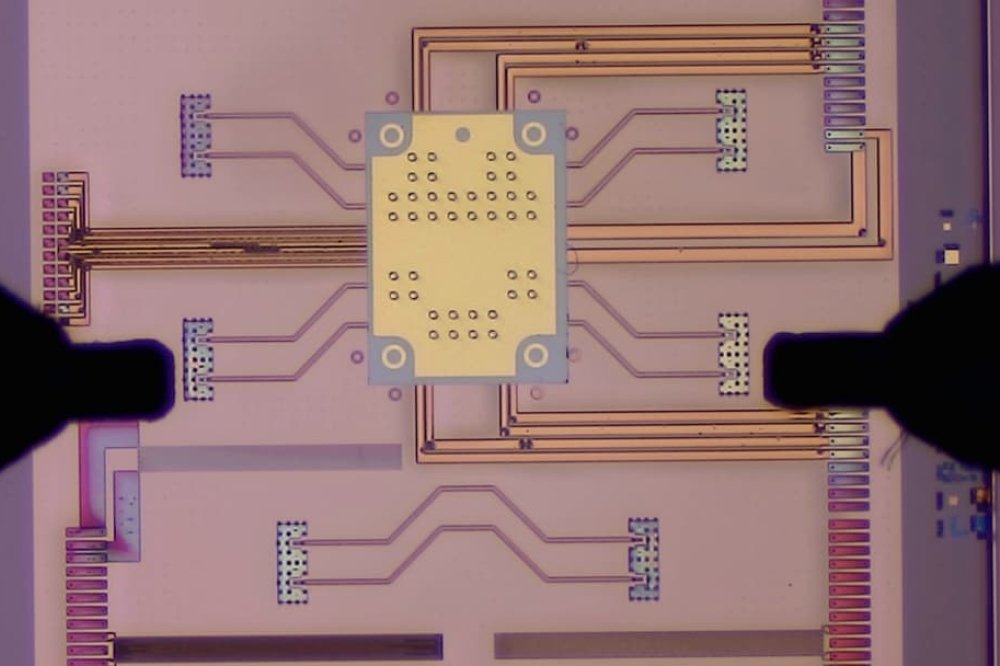
Figure 2: Several typical building blocks are needed in an Optical Network On Chip (ONoC). From left, these include: a ring modulator, a photodiode and an optical bus.
All device structures needed for on-chip optical networking are processed utilizing Silicon On Insulator (SOI) base wafers, within a standard process flow that includes silicon patterning, silicon doping (for light modulation and carrier collection) and local germanium epitaxy to build high speed photodiodes at the end of waveguides. Other available building blocks are ring filters, Mach-Zehnder modulators, multiplexers and power splitters. The process ends with a two-layer back end of line (BEOL) step for electrical wiring and a specific post process to grow the copper micropillars, with a typical pitch of 40 µm.
To give more flexibility to designers, LETI is also developing technological add-ons to the standard process flow, such as III-V material hybridization to form laser diodes on the Silicon Photonics platform, SiN to get ultra-low propagation loss waveguides, and TSV (through silicon vias) to enable electrical connection to the backside of the photonic interposer.
All these devices are designed to have a minimal footprint in order to be densely integrated in the optical interposer, to minimize the overhead with respect to the computation part of the chiplets. However, this computational power in the chiplet translates to electrical power and thermal dissipation by Joule effect. Microring modulators are temperature sensitive devices, which require an accurate thermal tuning to operate.
Leti recently demonstrated a digitally supervised thermal tuning architecture to control the local temperature of the microrings and lock to the laser wavelength. The transmission on the drop port of the microring allows monitoring the ring resonance and matching the optical power to a reference level, which optimizes the communication with a high extinction ratio and low insertion losses. This is done by means of an electro-optical analog feedback loop: the set point corresponds to an optical power value on the drop port; a photodiode converts this optical power to a photocurrent. A robust analog control loop tracks this photocurrent and drives a local heater near the microring to match the photocurrent against the reference. This brings all microring resonant wavelengths to the closest laser wavelength, and a specific data encoding in the transmission protocol allows identifying the actual wavelengths to recover the correct permutation of the data on the different wavelengths.
The thermal environment of the chip assembly is however very constrained, and it can evolve over time depending on the computation needs. In the case of a large temperature variation, maintaining the initial wavelength allocation on the WDM link can become sub-optimal in terms of Joule power, or could even become unfeasible without cooling down of the rings. Thus, a digital mechanism on top of the analog temperature-tracking loop fixes the set points to allow jumping from a laser wavelength to another. This needs to be done as fast as possible to minimize the unavailability of the data link. Overheat and under-heat thresholds are set on the heater power. When a threshold is reached, the feedback loop is changed from negative feedback to positive feedback to force the transition to a different edge of the resonance peak, and changed again to negative feedback to re-enable the communication on the next peak, as shown in Figure 3.
Figure 3: Shown above is an illustration of ways in which overheating and underheating are managed to continuously enable signal transmission within the ONoC.
Besides, the digital control forces some additional coordination between wavelengths, so that the full WDM channel remains operational. Nevertheless, this coordination is only done locally in each Tx or Rx, and the protocol maintains the communication whatever the mappings at source and destination. Given the temperature gradients across the chip assembly, this independence of the control between Tx's and Rx's is mandatory.
This approach has been successfully implemented on a silicon photonic network on chip prototype with a flip-chipped driver and thermal control electronics (ASIC).
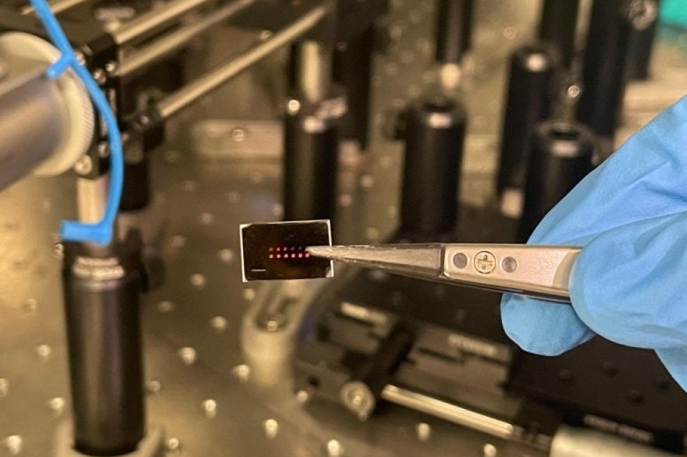
Figure 4: Electronic and photonic die are assembled together with microbump 3D connections, then electrical IOs are wirebonded to a board; a fiber array is then positioned above grating couplers. (Left) A close-up view of the silicon photonic network on chip prototype under test conditions designed to assess Leti's thermal management strategy. (Right) Board operation under optical prober in the lab.
This chip assembly implements a 4-wavelength WDM electro-optical link operational up to 10 Gbps per wavelength, with robust thermal control of microring resonances. The bottom die contains the silicon-photonic devices and waveguides, along with some metal redistribution layers, while the top die contains the electronic ASIC implemented in STMicroelectronics 65nm CMOS technology, with the 10 Gbps Tx and Rx drivers and the digitally supervised analog thermal control loops for all microrings. The dies are assembled using 3D Copper micropillars with a pitch of 40 μm. The electrical connection for one wavelength Tx or Rx uses 6 micropillars for modulation, photocurrent monitoring and heater control, i.e. a footprint of 96,000μm². The microring and photodiode as well as all the control and driving electronics at 10 Gbps fit within this footprint for an ultra-dense communication bandwidth of more than 1 Tbps/mm².
Measurements show that the temperature control allows maintaining the average optical power of the rings within 0.1 dB of the target set points of the modulators and filters, which corresponds to less than 0.5 pm error on the resonance wavelength. Starting from an off-resonance ring, the activation of the loop achieves locking on the resonance in 100 μs, which allows remapping the WDM optical link in 200 μs in case of a large temperature variation. Additionally, the control loop remains stable even when resonance variations occur around 1 kHz and 30 pm peak-to-peak, corresponding to a parasitic temperature variation of 0.5 K at a change rate observable during processor activity.
These efforts have demonstrated that high-density integration of optical communication channels are possible, renewing the roadmap of high-bandwidth 2.5D interposers for high performance computers. They open the way to large scale optical integration of manycore processors on a photonic interposer implementing an optical network on chip. Such an ONoC would allow a scale-up of 2-4à— in processor count with multiple Terabytes/s aggregate bandwidth for lower latencies than CMOS interposers while maintaining the same power envelope for on-chip/on-board communication.


