Photonic integrated comb sources enable high volume applications

An optical comb source is a laser that produces a spectrum consisting of multiple equidistant frequencies. The huge potential of optical comb lasers was recognised in 2005, when they were the subject of the Nobel Prize for Physics, an accolade reserved for highly disruptive discoveries, efforts and inventions. The prize was awarded to John L. Hall and Theodor W. Hänsch "for their contributions to the development of laser-based precision spectroscopy, including the optical frequency comb technique".
Optical combs have been demonstrated as useful tools to enhance a diverse range of applications including precision spectroscopy, microwave synthesis, frequency metrology, optical clocks, and communications.
At its simplest, an optical comb can be used to replace an array of independent lasers, like those of a wavelength division multiplexed (WDM) communications system. However, it is their more subtle properties; the coherence of the comb lines, and the precision of the frequency spacing between them, that create new possibilities and offer unique advantages over existing laser sources.
While the promise of comb lasers has been recognised, most commercial optical comb sources have been the preserve of scientists to date; they are expensive pieces of laboratory equipment which has limited their use in high volume applications.
Recent advances in photonic integration have enabled several demonstrations of on-chip optical combs that have the potential to open up volume markets for the first time. Opportunities for combs are found in optical communications, low cost optical sensing for the internet of things, and chip-scale atomic clocks that can benefit from photonic integrated optical combs.
Comb generation techniques
Optical combs can be generated using many different techniques, and the suitability of each depends on the application.
They can be generated via mode-locking, in either solid-state (including fibre), or diode laser cavities. The solid-state type is the most widely deployed commercial comb source and offers excellent optical properties and a wide comb bandwidth. They are an excellent choice for laboratory and scientific work, but are less suited to low-cost, high-volume applications.
Mode-locked laser diodes on the other hand, do offer the potential for photonic integration. They have been explored deeply in the research community, for example through the EU FP7 project Big Pipes [1], and they are being actively commercialised for short reach communications.
A draw-back of mode-locked techniques in general is that they are based on a fixed physical cavity, and therefore the comb spacing is generally static. This limits swept-mode operation which can prove useful in applications such as spectroscopy and frequency metrology.
Optical combs can also be generated by over-driving electro-optic modulators. In order to get a high quality comb, numerous modulators (each requiring their own RF driver,) are typically used in series. This drives up the cost of the comb source, and also increases the optical loss, often necessitating the use of an optical amplifier which also limits commercial applicability.
Comb generators based on the Kerr effect in ring resonators are receiving much attention and many impressive results have been published recently on optical combs based on micro ring resonators. The efficiency of such devices can prove challenging, with external high-power pump lasers or amplifiers often required. However, more efficient devices, requiring less optical pump power are being actively developed, which provide excellent potential for low-cost commercial devices over time [2,3,4].
The reader is referred to the following references [5,6,7,8] for several far more detailed surveys and reviews of the various types and applications of optical combs. The remainder of this article focuses on gain switched comb generation from a monolithically integrated photonic chip a technique that offers a balance of simplicity, flexibility and performance.
Gain switched comb generation
The gain switching technique was originally used for short optical pulse generation. A semiconductor laser is directly modulated with a sine wave generating a series of short optical pulses with a repetition rate that is set by the frequency of the drive signal. Because the light in the laser cavity is completely extinguished during gain switching, the pulses are incoherent and therefore in the frequency domain, a broad continuous spectrum is observed. The use of an additional "master" laser to injection lock the gain switched "slave" laser can ensure that there is always light in the cavity, increasing the pulse to pulse coherence, and resulting in the set of discrete frequency tones that make up an optical comb.
The separation of the continuous wave (CW) master and modulated slave laser provides additional benefits. Through injection locking, the properties of the master laser including its linewidth are imparted on all of the comb lines. This offers the opportunity to optimise its parameters for optical quality, while optimising the slave for gain switching.
The ability to set the wavelength spacing using an RF frequency, as opposed to having it determined by a physical cavity, provides some of the key benefits of gain switched combs. With mode-locked diode lasers for example, the comb spacing accuracy is governed by the accuracy of the facet cleave and is often in the gigahertz range. In contrast, comb spacings accurate to sub-kHz levels can be achieved using gain switching. Furthermore, the distance between the comb lines can be swept with high accuracy and speed, enhancing applications such as spectroscopy and fibre sensing where swept wavelength tunable laser sources are regularly used to interrogate samples or sensors. This concept is illustrated in Figure 1.
Figure 1: A sawtooth wave is used to sweep the voltage controlled oscillator that sets the comb spacing. One tone is locked in frequency by the master laser, while all other tones spread out from that point, as the comb frequency spacing is swept. In the example shown, a frequency discriminator consisting of an optical filter and a photodetector is used to capture the wavelength sweep.
Integrating the comb with active optical filtering for advanced applications
By integrating the master and slave lasers on a single chip, a photonic integrated comb source less than one square millimetre in footprint can be produced, while the electronics required to drive it are simple, and low-cost. Efforts are currently underway to produce optoelectronic comb source modules at prices and in form-factors typical of high-volume optical transceivers.
From this core building block of the comb PIC, even more powerful application specific PICs can be created through the integration of other components and structures. Active optical filters that allow one or more of the comb lines to be extracted and used for frequency shifting, frequency multiplication, frequency generation, or for modulating individual comb-lines with data are of particular importance. Three examples of the many applications enabled by this exciting technology are briefly described below.
Frequency metrology
By using integrated optical filters to select any two lines from a comb with tunable frequency spacing, an extremely versatile microwave, millimetre-wave, and sub-THz frequency generator can be created. An exciting application of this approach is in coherent population trapping (CPT), a technique used in rubidium atomic clocks. The photonic integrated comb architecture can be used to generate an optical signal consisting of just two coherent modes, spaced by the rubidium atomic resonance frequency, and centred on its absorption peak. By illuminating a vapour cell containing rubidium atoms and feeding back control signals from the detected light to the comb source, an atomically stable clock signal can be generated. Space agencies, academic researchers and commercial aerospace corporations are excited by the potential of this novel approach.
Optical networking
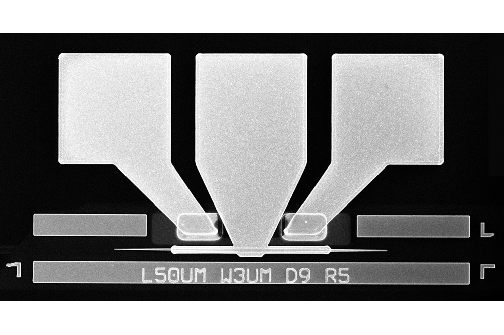
Almost all of the highest capacity, highest spectral efficiency optical transmissions ever carried out are based on optical combs, and yet, to date no comb-based coherent transceiver has made it to market. Today's coherent transceivers employ one, or in some cases two optical carriers produced by independent lasers. Going beyond that to four or even eight wavelengths for terabit coherent transceivers poses cost, power and footprint challenges and comb sources have a role to play here. A key challenge has been the need to split the comb lines onto individual waveguides or fibres for data modulation, in a cost, size, and power efficient way. By monolithically integrating a gain switched comb source with a four or eight channel active optical filter, an on-chip demultiplexer can be created which separates the comb lines, amplifies them for external modulation and improves the carrier to noise ratio, while retaining the coherence between the lines. This disruptive technology makes optical combs a viable option for coherent transceivers for the first time, and is gaining the attention of several optical equipment vendors. (See Figures 2a and 2b)
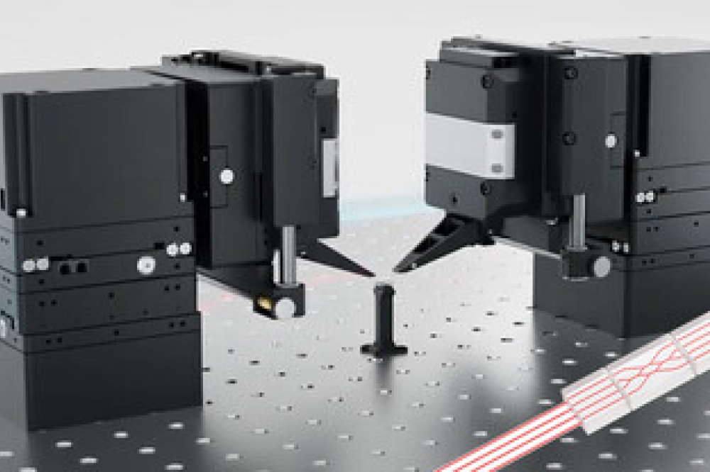
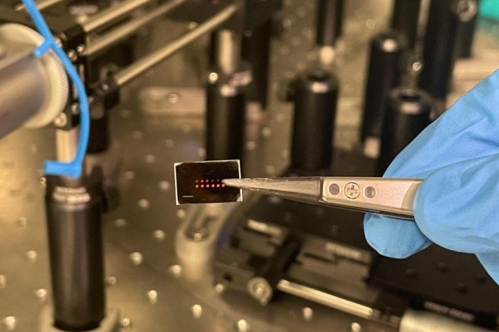
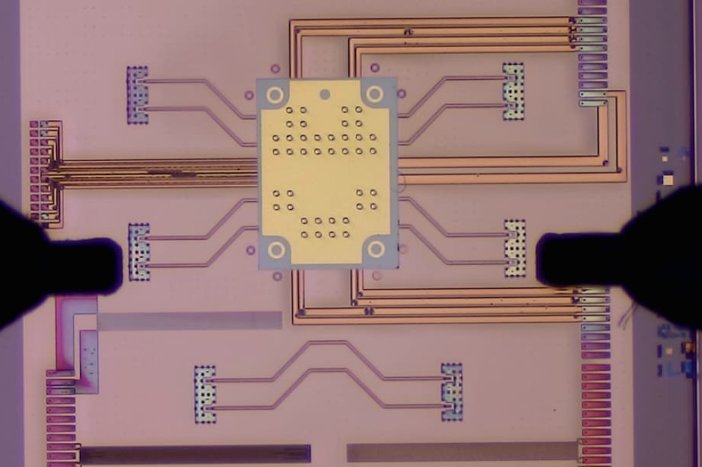
Figure 2a (left) and Figure 2b(right) : (a) Pilot Photonics monolithically integrated comb source and demux PIC makes combs suitable for use in coherent optical transcievers for the first time. Ideally suited to 400G and 1T coherent transceivers, the chip delivers four coherent comb tones to separate fibers for modulation with data. (b) The chip and RF driver are co-packed in a high-speed optical package and light is coupled out using a four fiber array, allowing a single optical package to replace four individual laser packages that are used in typical transceivers. The Pilot Photonics device readily scales to greater channel counts.
Optical fibre sensing and spectroscopy
A third high-volume application of integrated optical combs is in dual comb spectroscopy, a powerful technique that uses two slightly offset combs to interrogate a sample, or a sensor. The benefits of dual-comb spectroscopy are that it provides a near real-time, high-resolution spectral output without any requirement for laser tuning. In effect, it transposes an optical measurement problem to the RF domain. Dual gain switched comb sources can easily be generated on a single chip, and an example is shown below. By coupling the power of the dual-comb technique with the cost and size benefits of photonic integration this architecture can unleash the potential of optical sensing by increasing the performance while reducing the cost and complexity of the laser systems required.
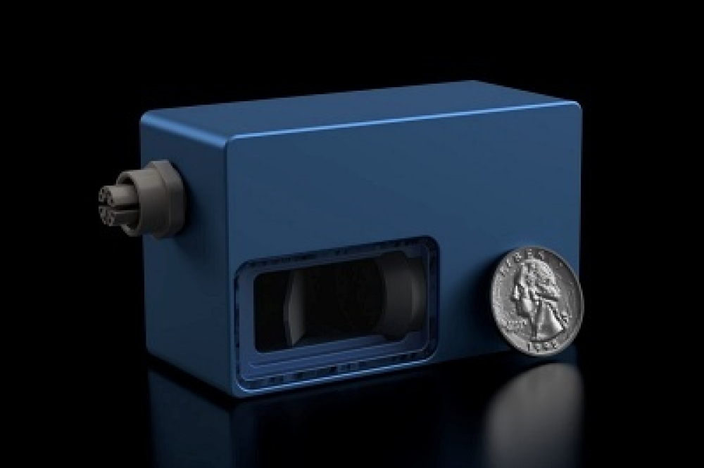
Figure 3: Pilot Photonics' dual-comb Lyra-OCS-1000 is shown above
Pilot Photonics Lyra-OCS-1000 is the most cost-effective comb source on the market. Offering one-touch operation, it delivers a flexible gain switched comb from a fully integrated opto-electronic module.
Conclusion
Optical combs have been duly recognised as one of the most important technologies of our time as they form a bridge between the RF and optical worlds. Their intersection with photonic integration creates wonderful possibilities and offers the potential for truly disruptive innovation, which will see their widespread deployment in numerous high-volume applications. Gain switched comb generation is a powerful and versatile approach that offers the potential for ultra-low cost implementation. (Figure 3) If you have an application to which it could be applied, please get in touch with Pilot Photonics.


