Extreme conditions in semiconductors
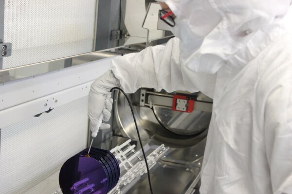
Scientists from the University of Konstanz and Paderborn University have succeeded in producing and demonstrating what is known as Wannier-Stark localisation for the first time in a high-purity GaAs crystal grown at ETH Zurich.
In doing so, the physicists managed to overcome obstacles that had so far been considered insurmountable in the field of optoelectronics and photonics.
Wannier-Stark localisation causes extreme imbalance within the electric system of crystalline solids. "This fundamental effect was predicted more than 80 years ago. But it has remained unclear ever since whether this state can be realised in a bulk crystal, that is, on the level of chemical bonds between atoms", says Alfred Leitenstorfer, professor of Experimental Physics at the University of Konstanz.
Analogues of the effect have so far been demonstrated only in artificial systems like semiconductor superlattices or ultracold atomic gases. In a bulk solid, Wannier-Stark localization can only be maintained for an extremely short period of time, shorter than a single oscillation of infrared light. Using the ultrafast laser systems at the University of Konstanz, Wannier-Stark localization has now been demonstrated for the first time. The experiment was conducted in a high-purity GaAs crystal grown at ETH Zurich using epitaxial growth. The research results were published in Nature Communications on 23 July 2018.
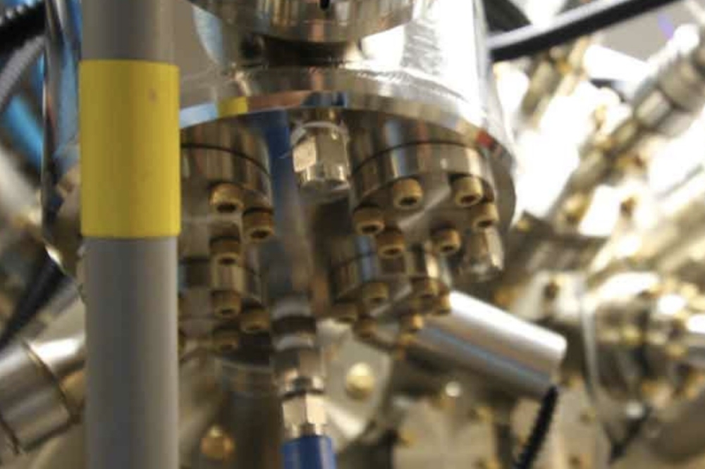
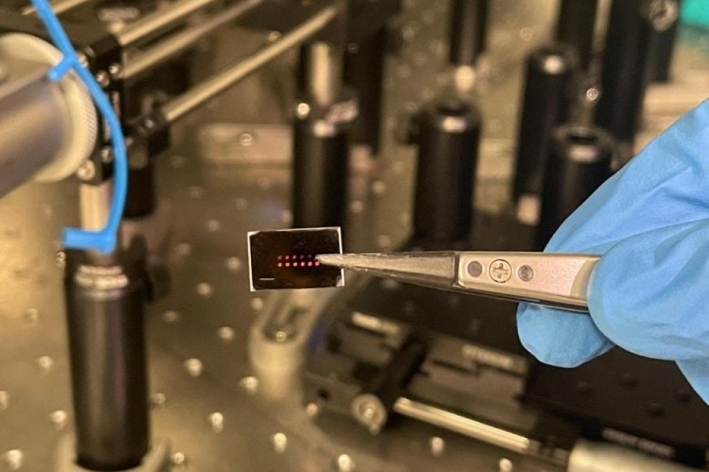
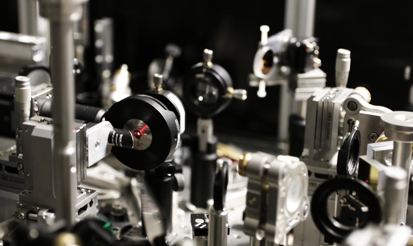
The picture above is a close-up of the experimental setup in the University of Konstanz's high-field Terahertz lab. Under the extreme conditions of the experiment, a bright red glow can be seen to emanate from the GaAs crystal used as a semiconductor. This is due to the system's extremely high optical nonlinearity, which occurs when Wannier-Stark localisation sets in.
What is Wannier-Stark localisation?
If we tried to picture the atoms of a crystal, it would have to be as a three-dimensional grid composed of small beads that repel each other and are only kept together by rubber bands. The system remains stable as long as the rubber band is as strong as the repulsion is. If this is the case, the beads neither move closer to each other, nor do they move away from each other - the distance between them remains about the same. Wannier-Stark localisation occurs when the rubber bands are removed abruptly.
It is the electronic state that happens at the precise moment in time when the rubber bands have already gone but the beads still remain in place: The chemical bonds that hold the crystal together have been suspended.
If this state is maintained for too long, the beads will break apart and the crystal dissolves. To analyze Wannier-Stark localszation, the physicists had to remove the stabilising structures, capture the system within a fraction of a light oscillation using light pulses, and finally to stabilise it again to prevent the atoms from breaking apart.
The experiment was made possible through the highly intense electric field of an ultrashort infrared light pulse, which is present in the crystal for a few femtoseconds only. "This is what we specialise in: studying phenomena that only exist on very short time scales", explains Alfred Leitenstorfer.
"In perfect insulators and semiconductors, electronic states expand throughout the entire crystal. According to an 80-year-old prediction, this changes as soon as electrical voltage is applied", says Torsten Meier from Paderborn University. "If the electric field inside the crystal is strong enough, the electronic states can be localised to a few atoms. This state is called the Wannier-Stark ladder", explains the physicist, who is also Vice-President for International Relations at Paderborn University.
New electronic characteristics
"A system that deviates so extremely from its equilibrium has completely new characteristics", says Alfred Leitenstorfer about why this state is so interesting from a scientific perspective. The short-lived Wannier-Stark localisation correlates with drastic changes to the electronic structure of the crystal and results, for example, in extremely high optical nonlinearity. The scientists also assume that this state is chemically particularly reactive.
The first-ever experimental realisation of Wannier-Stark localisation in a GaAs crystal was made possible through highly intense Terahertz radiation with field intensities of more than ten million volts per centimetre. The application of more ultrashort optical light pulses resulted in changes to the crystal's optical characteristics, which was instrumental to proving this state.
"If we use suitably intense light pulses consisting of a few oscillations lasting some ten femtoseconds only, we can realize the Wannier-Stark localisation for a short period of time", says Alfred Leitenstorfer. "Our readings match the theoretical considerations and simulations carried out both by my own research team and by that of my colleague, Professor Wolf Gero Schmidt", adds Torsten Meier. The researchers are planning to study the extreme state of Wannier-Stark localisation on the atomic scale in more detail in the future and intend to make its particular characteristics usable.
'Signatures of transient Wannier-Stark localization in bulk gallium arsenide' by C. Schmidt et el; Nature Communications 9, 2890 (2018)


