IQE reaches NIL production milestone

IQE has announced that its proprietary NanoImprint Lithography (NIL) technology has reached a significant milestone. The new technology offering has been production qualified by a leading supplier of DFB lasers into the telecoms industry, and the first production order for $250,000 has been received. Production will commence immediately.
DFB lasers are high performance edge emitting (EE) lasers that are critical enabling transmission components for high-speed data communications across the whole fibre optic network. Exponential future demand for DFBs in this sector will be driven by 5G connectivity and the adoption of Internet of Things.
In addition, the high optical quality of the DFB device makes it the edge emitting laser of choice for the commoditisation of a wide range of emerging sensing applications such as 3D sensing, environmental emissions and air quality monitoring, chemical weapons and explosives detection, and disease diagnosis via breath and blood vessel monitoring.
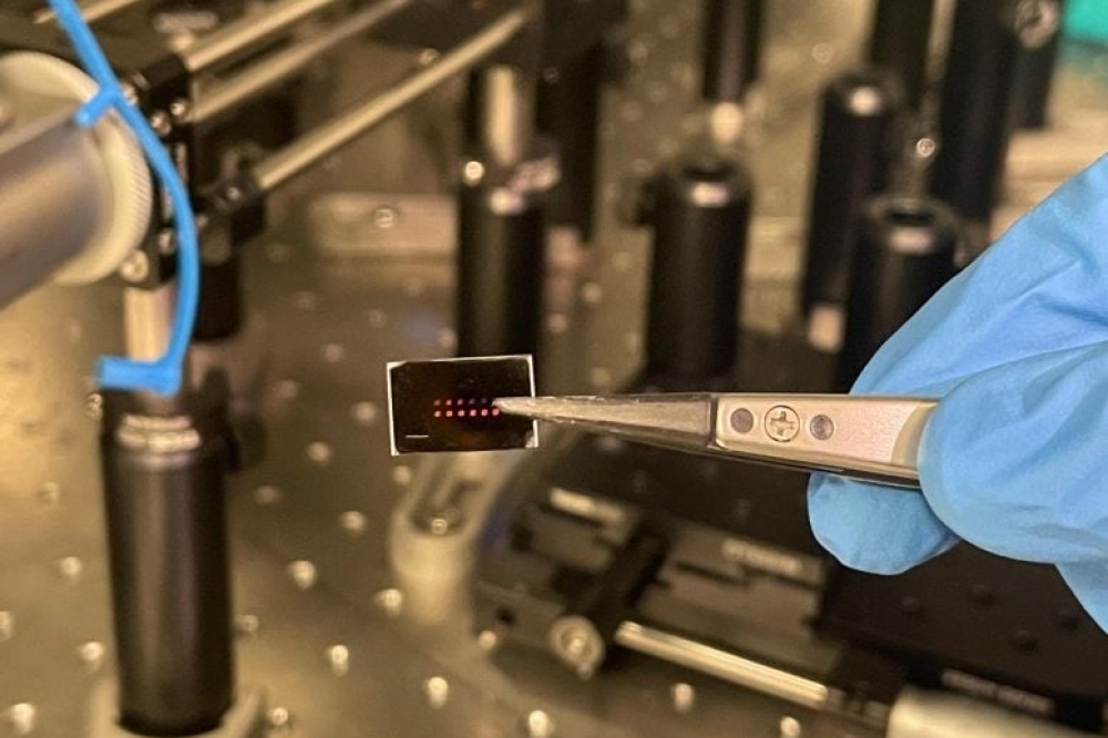
NanoImprint Lithography is a powerful technology for the large scale and low-cost manufacture of submicron features in a variety of materials, including compound semiconductors, silicon, glass, oxides and flexible materials such as polymers. IQE says its technology is capable of achieving the complex patterns typically produced using expensive and slow throughput e-beam lithography, but at a much lower cost and much higher throughput.
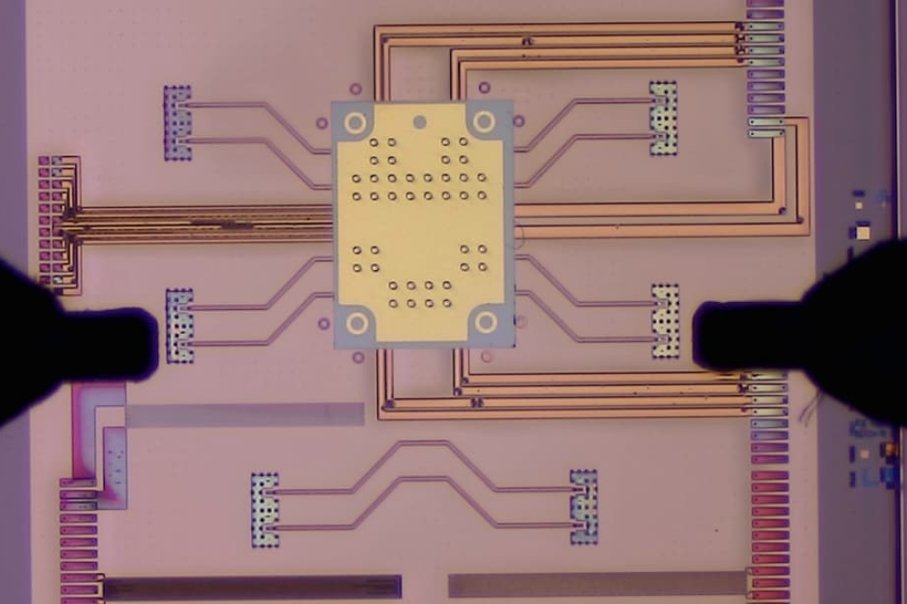
Applications include a multitude of photonics products, including gratings for DFB lasers, Micro and Patterned Sapphire Substrate (PSS) LEDs, Diffractive Optical Elements (DOE), and QuasiPhotonic Crystals.
With respect to the current DFB application, IQE's customer has found that using the NIL gratings provides greater precision and dimensional control (which have resulted in higher performance in side mode suppression ratio (SMSR), a key performance measure of DFB lasers), better pitch and duty cycle uniformity, and narrower lasing wavelength within the wafer for the customer as compared to conventional interference holography. All other performance characteristics were similar or better than the conventional holographic production.
Rodney Pelzel, VP global technology for IQE commented: "This production qualification marks a significant milestone in the introduction of IQE's proprietary NanoImprint Lithography technology into the mainstream telecoms industry.
"Coupled with a wide range of new and exciting technologies such as crystalline Rare Earth Oxides (cREO) and Quasi-Photonic Crystals, which are also manufactured using the NanoImprint Lithography technology, IQE's IP portfolio is gaining significant traction, allowing the company to offer new, disruptive technologies to the broad semiconductor marketplace."
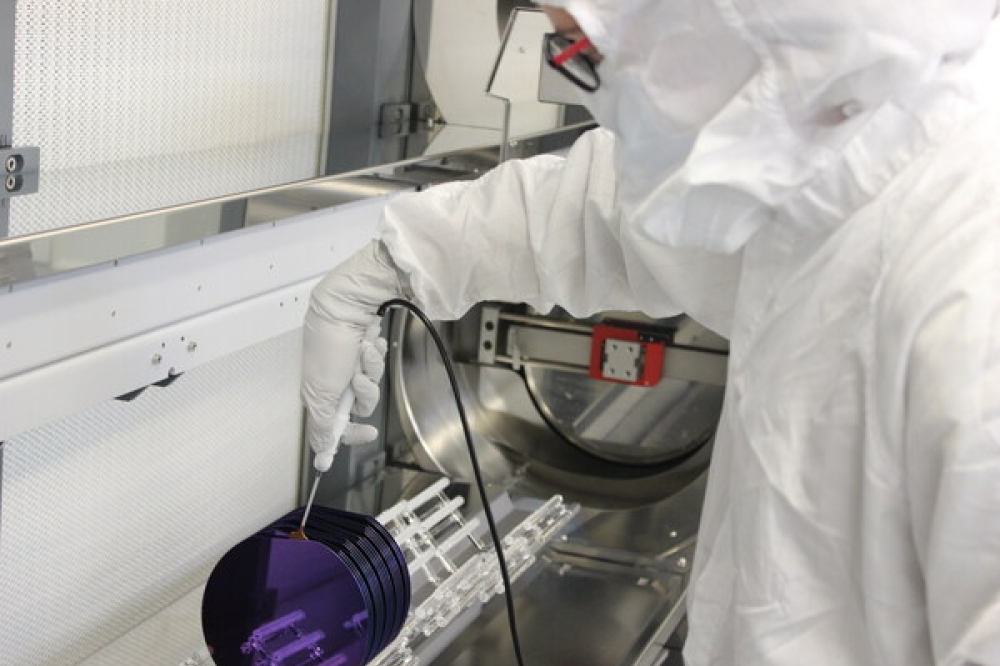
NanoImprint Lithography is suited for mass manufacture of wafers at 100mm, 150mm, 200mm sizes, and can even be scaled to 300mm. In addition to DFB applications, IQE is also currently engaged in multiple other qualification programmes incorporating the Nanoimprint Lithography technology across a range of wafer sizes and end applications.


