Loading...
News Article

Oxford Plasma Tech tool used for novel opto detector

News
Researchers at AMO have used Oxford Instruments Plasma Technology's fabrication solutions to develop a graphene based photonics device capable of operating at 25 Gb/s per channel

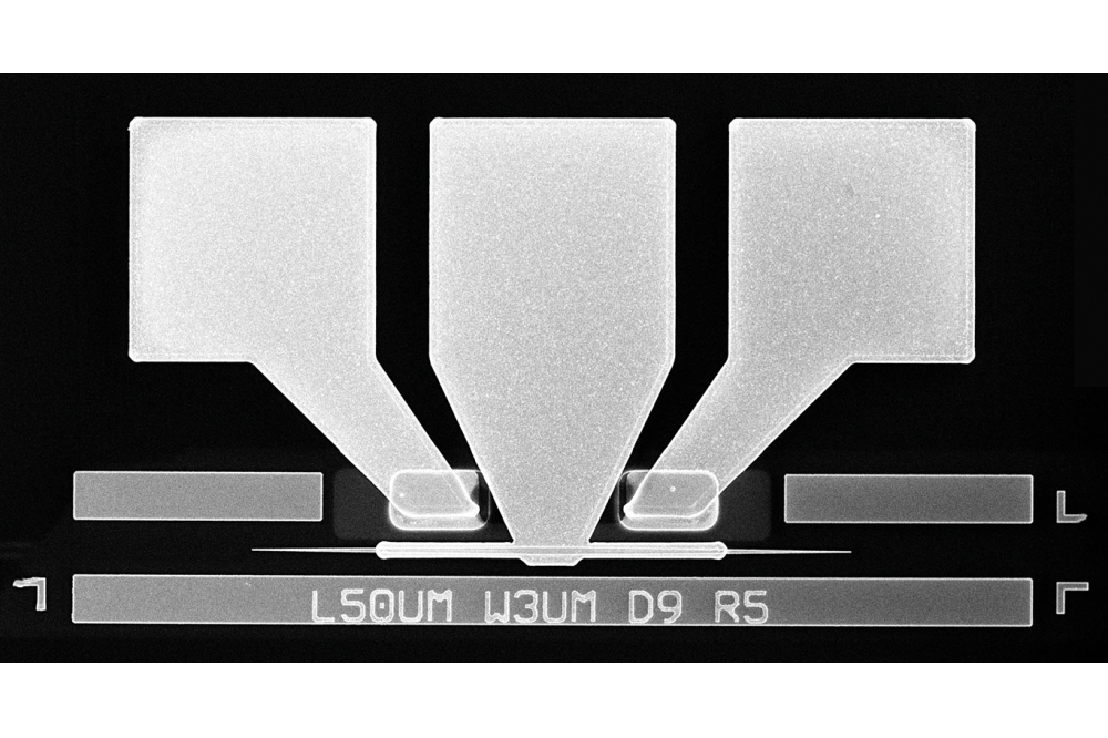
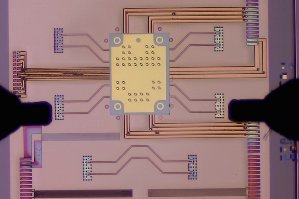
Researchers at AMO GmbH, a non-profit SME based in Aachen, have used Oxford Instruments Plasma Technology's fabrication solutions to develop a graphene based photonics detector device capable of operating at a data rate of 25 Gb/s per channel. The device converts optical modulation data into an electrical signal.

Oxford Instruments offers solutions for the data communications market for both scaled-up production as well as novel device R&D. The detector fabrication solution includes: waveguide fabrication, III-V/2D materials mesa etching and graphene/2D/novel materials deposition. In addition Oxford Instruments also offers a range of solutions for devices such as the InP edge emitting lasers and VCSELs for photonic data communications.

Devices developed by scientists at AMO within the European Graphene Flagship project have set the yardstick in terms of high speed photodetectors operating at telecom wavelengths. At the Mobile World Congress in Barcelona this year, AMO scientists along with collaborators with the Graphene Flagship project demonstrated the world's first graphene data communication link operating at 25 Gbits/s per channel. As such the detector developed at AMO can reach speeds of up to 130 GHz

"We are extremely delighted to see the progress made by researchers at AMO on our device fabrication solutions", says Frazer Anderson, innovation and solutions director, Oxford Instruments Plasma Technology. He continued:" We continue to invest in further developing and improving our cutting edge device fabrication processes for datacomms and photonics through feedback from such impressive success stories."

Max Lemme, managing director, AMO GmbH comments: "The latest results on high-speed graphene-based data communication are very encouraging. They are a positive testament to AMO's mission: to identify new materials and to demonstrate new technologies for future applications in electronics and optoelectronics, such as IOT and 5G. We can only achieve such results through our state-of-the-art R&D process line, which includes a large number of tools for scalable nanotechnologies, such as Oxford Instruments' RIE, ALD and CVD tools"

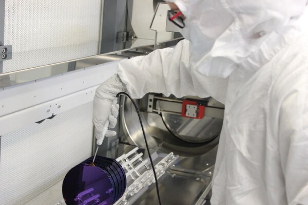
The devices were developed at AMO's 6inch device fabrication pilot line equipped with Oxford Instruments fabrication solutions which includes ICP RIE, ALD and PECVD tools.

Quintessent appoints Bob Nunn chief operating officer
PI to demonstrate new PIC alignment system at Photonics West
Drut launches 2500 product series with CPO for AI datacentres
III-V Epi advocates GaAs for new lasers
Marvell announces new CPO architecture for custom AI accelerators
Printing high-speed modulators on SOI
Photon IP raises €4.75m for advanced PICs
ANELLO Photonics launches Maritime Inertial Navigation System
Aeluma joins AIM Photonics as full industry member
Imec makes breakthrough with GaAs lasers on silicon
POET acquires Super Photonics Xiamen
Voyant Photonics launches affordable Carbon LiDAR
Penn State makes breakthrough in photonic switching
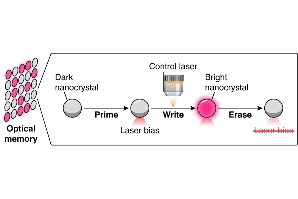
New nanocrystals could lead to more efficient optical computing
QCi awarded NASA contract to apply Dirac-3 photonic optimisation solver
The Netherlands launches ChipNL Competence Centre
TOPTICA to create chip-integrated lasers for quantum PIC project
NSF selects six pilot projects for National Quantum Virtual Laboratory
SiLC Technologies launches Eyeonic Trace Laser Line Scanner
Southwest Advanced Prototyping Hub awarded $21.3 million CHIPS Act funding
Cambridge Graphene Centre and CORNERSTONE to participate in PIXEurope
Cost-effective lasers for extended SWIR applications
IBM unveils co-packaged optics technology for AI and datacentres
QCi announces $50 million concurrent stock offerings
CHIPS Act funding to be awarded to Coherent, Skywater, and X-Fab
ERC consolidator grant awarded for optoacoustic neural network project
Imec demonstrates InP chiplet integration on 300 mm RF silicon interposer
Ayar Labs raises $155 million for optical I/O
Celestial AI awarded 2024 Start-up to Watch by Global Semiconductor Alliance
Researchers develop “last missing piece” of silicon photonics
Quantum sensors for controlling prosthetics
UPVfab to participate in European Commission photonic chips project

×
Search the news archive

To close this popup you can press escape or click the close icon.
Logo
x
Logo
×
Register - Step 1

You may choose to subscribe to the PIC Magazine, the PIC Newsletter, or both. You may also request additional information if required, before submitting your application.


Please subscribe me to:


You chose the industry type of "Other"

Please enter the industry that you work in: