
NIST team shrinks photonic chip for precision spectroscopy
A prototype photonic chip developed by a research team at the US National Institute of Standards and Technology (NIST) could provide the basis for a future generation of extremely compact quantum sensors.
The researchers, working under the "NIST-on-a-chip" initiative, say they have created a chip upon which near-infrared laser light interacts with a tiny cloud of atoms, the basis for measuring quantities such as length with quantum precision.
They also believe that current weaknesses in the design can be overcome with some minor tweaks, and that tiny precision spectrometers based on their approach could be mass-produced using existing semiconductor wafer manufacturing technology.
Length reference
Describing the work in the journal Optica, Matt Hummon and colleagues report that the NIST prototype generates 780 nm light with sufficient precision (10-11 instability) to act as a length reference for calibrating other instruments through interaction with rubidium atoms.
"This device harnesses the benefits of both photonic integration and precision spectroscopy for the next generation of quantum sensors and devices based on atomic vapors," wrote the team in their paper.
And although the stability of the current prototype is limited by thermal drifts of etalons created by back-reflections in the chip's waveguide, that could be overcome by using a larger probe beam, or a narrower optical transition.
"Thus, we expect that future photonic chip designs that reduce the etalons generated by the back-reflections in the waveguide will lead directly to improved frequency stability," concludes the team. "Wafer-level mass fabrication of both the micro-machined vapor cells and the photonic chips may lead to inexpensive devices based on precision spectroscopy of warm vapors."
While a quantum sensor based around an atomic vapor typically requires fridge-sized equipment, recent developments in the UK have shown that it is possible to shrink that volume down by an order of magnitude, suitable for integration within a "CubeSat" format.
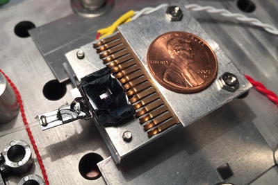
The NIST prototype takes that much further, packing the atom cloud and structures for guiding light into an area of less than a square centimeter: a remarkable four orders of magnitude smaller than current macro-sized sensors offering similar measurement precision.
The reported chip measures just 14 mm long by 9 mm wide, with its silicon nitride waveguides able to handle a wide range of light frequencies.
"Compared to other devices that use chips for guiding light waves to probe atoms, our chip increases the measurement precision a hundred-fold," added Hummon. "Our chip currently relies on a small external laser and optics table, but in future designs we hope to put everything on the chip."
Novel waveguide and grating
Applications of such a device could include measuring quantities such as
time, length and magnetic field strength, with potential for deployment
in navigation, communications, and medical equipment.
Critical to the tiny structure are a novel waveguide and grating, which expand the beam diameter to excite approximately 100 million atoms into a higher energy level.
In the current design, the NIST team used rubidium atoms, but in principle the approach could work with a wide range of atomic and molecular vapors to generate specific frequencies across the visible and near-infrared spectrum.
Perhaps most significantly, the chip is unlike current high-precision sensors in that it could be mass-produced in a similar manner to a semiconductor wafer. Conventional systems instead require manual assembly of bulky optics and blown-glass vapor cells, according to NIST group leader John Kitching.
The NIST paper indicates frequency metrology with a precision error of 1 part error in 10 billion at 100 seconds "“ with that performance verified by comparison with a separate NIST frequency comb.
"This performance level is very good for something so small, although full-scale lab instruments are more precise," Kitching said.
Getting out of the lab
The "NIST-on-a-chip" program is intended to move new metrology
technologies out of the preserve of the specialist laboratory, and into
commercial markets where they can be manufactured by the private sector,
and deployed directly by users.

"To that end, we are developing a suite of intrinsically accurate, quantum-based measurement technologies intended to be deployed nearly anywhere and anytime, performing uninterrupted without the need for NIST's traditional measurement services," states NIST.
"They will enable users to make precision measurements referenced to the International System of Units (SI) on factory floors, in hospital diagnostic centers, in commercial and military aircraft, in research labs, and ultimately in homes, automobiles, and personal electronic devices, among others."
With projects across 12 different technology areas planned, photonics technology is a key element in many. Among the novel ideas are "photonic thermometers", which would sense changes in the size and thermal profile of an object to measure temperature, in place of a traditional mercury instrument.


