
Integrating optical components into existing chip designs
Technique would allow addition of optical communication components to existing chips with little modification of their designs.
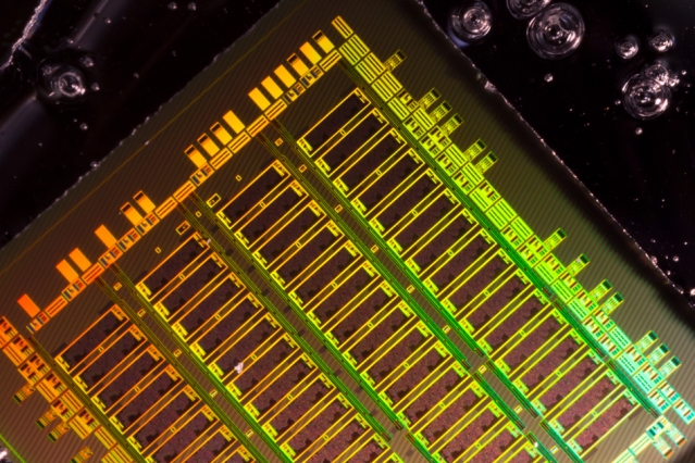
Image: Amir Atabaki
Two and a half years ago, a team of researchers led by groups at MIT, the University of California at Berkeley, and Boston University announced a milestone: the fabrication of a working microprocessor, built using only existing manufacturing processes, that integrated electronic and optical components on the same chip.
The researchers' approach, however, required that the chip's electrical components be built from the same layer of silicon as its optical components. That meant relying on an older chip technology in which the silicon layers for the electronics were thick enough for optics.
In the latest issue of Nature, a team of 18 researchers, led by the same MIT, Berkeley, and BU groups, reports another breakthrough: a technique for assembling on-chip optics and electronic separately, which enables the use of more modern transistor technologies. Again, the technique requires only existing manufacturing processes.
"The most promising thing about this work is that you can optimize your photonics independently from your electronics," says Amir Atabaki, a research scientist at MIT's Research Laboratory of Electronics and one of three first authors on the new paper. "We have different silicon electronic technologies, and if we can just add photonics to them, it'd be a great capability for future communications and computing chips. For example, now we could imagine a microprocessor manufacturer or a GPU manufacturer like Intel or Nvidia saying, "˜This is very nice. We can now have photonic input and output for our microprocessor or GPU.' And they don't have to change much in their process to get the performance boost of on-chip optics."
Light appeal
Moving from electrical communication to optical communication is attractive to chip manufacturers because it could significantly increase chips' speed and reduce power consumption, an advantage that will grow in importance as chips' transistor count continues to rise: The Semiconductor Industry Association has estimated that at current rates of increase, computers' energy requirements will exceed the world's total power output by 2040.
The integration of optical "” or "photonic" "” and electronic components on the same chip reduces power consumption still further. Optical communications devices are on the market today, but they consume too much power and generate too much heat to be integrated into an electronic chip such as a microprocessor. A commercial modulator "” the device that encodes digital information onto a light signal "” consumes between 10 and 100 times as much power as the modulators built into the researchers' new chip.
It also takes up 10 to 20 times as much chip space. That's because the integration of electronics and photonics on the same chip enables Atabaki and his colleagues to use a more space-efficient modulator design, based on a photonic device called a ring resonator.
"We have access to photonic architectures that you can't normally use without integrated electronics," Atabaki explains. "For example, today there is no commercial optical transceiver that uses optical resonators, because you need considerable electronics capability to control and stabilize that resonator."
Atabaki's co-first-authors on the Nature paper are Sajjad Moazeni, a PhD student at Berkeley, and Fabio Pavanello, who was a postdoc at the University of Colorado at Boulder, when the work was done. The senior authors are Rajeev Ram, a professor of electrical engineering and computer science at MIT; Vladimir Stojanovic, an associate professor of electrical engineering and computer sciences at Berkeley; and Milos Popovic, an assistant professor of electrical and computer engineering at Boston University. They're joined by 12 other researchers at MIT, Berkeley, Boston University, the University of Colorado, the State University of New York (SUNY) Polytechnic Institute, and Ayar Labs, an integrated-photonics startup that Ram, Stojanovic, and Popovic helped found.
Sizing crystals
In addition to millions of transistors for executing computations, the researchers' new chip includes all the components necessary for optical communication: modulators; waveguides, which steer light across the chip; resonators, which separate out different wavelengths of light, each of which can carry different data; and photodetectors, which translate incoming light signals back into electrical signals.
Silicon "” which is the basis of most modern computer chips "” must be fabricated on top of a layer of glass to yield useful optical components. The difference between the refractive indices of the silicon and the glass "” the degrees to which the materials bend light "” is what confines light to the silicon optical components.
The earlier work on integrated photonics, which was also led by Ram, Stojanovic, and Popovic, involved a process called wafer bonding, in which a single, large crystal of silicon is fused to a layer of glass deposited atop a separate chip. The new work, in enabling the direct deposition of silicon "” with varying thickness "” on top of glass, must make do with so-called polysilicon, which consists of many small crystals of silicon.
Single-crystal silicon is useful for both optics and electronics, but in polysilicon, there's a tradeoff between optical and electrical efficiency. Large-crystal polysilicon is efficient at conducting electricity, but the large crystals tend to scatter light, lowering the optical efficiency. Small-crystal polysilicon scatters light less, but it's not as good a conductor.
Using the manufacturing facilities at SUNY Polytechnic Institute's Colleges of Nanoscale Sciences and Engineering, the researchers tried out a series of recipes for polysilicon deposition, varying the type of raw silicon used, processing temperatures and times, until they found one that offered a good tradeoff between electronic and optical properties.
"I think we must have gone through more than 50 silicon wafers before finding a material that was just right," Atabaki says.


