
Light Exposure Significantly Impacts Crystal Elasticity
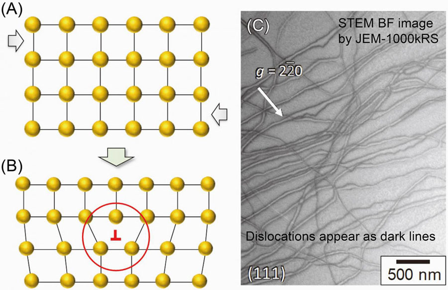
Plastic deformation of crystalline materials is caused by nucleation and multiplication of dislocations under an external force (A and B). It has been generally believed that brittle inorganic semiconducting materials have difficulty in formation of dislocations because of their strong chemical bonds. However, researchers found that a great number of dislocations are generated and multiplied in ZnS crystals during deformation in darkness (C), resulting in the extraordinary plasticity that researchers observed. Image courtesy of Atsutomo Nakamura.
Researchers at Nagoya University have found that inorganic semiconductors become brittle when exposed to light but remain comparatively flexible when kept in the dark at room temperature. This finding could have significant impact upon semiconductor and optoelectronic device manufacturing due to the fact that brittleness of underlying crystal lattices can limit applications of traditional silicon and other crystalline substrates in flexible electronics; cracks in semiconductor die often lead to premature device failures or can shorten servicable product lifetimes.
The university researchers studied the deformation of zinc sulfide (ZnS) crystals under white light, UV light, and in complete darkness. Microscopy revealed that under the two light conditions the inorganic semiconducting material immediately cracked when researchers attempted to deform it. In contrast, the ZnS was able to withstand substantial deformation "” up to 45 percent "” when kept in complete darkness. The results suggest that the strength, brittleness, and conductivity of inorganic semiconductors could be regulated by light exposure, opening a possible avenue to optimize the performance of inorganic semiconductors in electronic and in optoelectronic applications.Their results were published in the current edition of Science magazine.
The team attributed the increased plasticity of the ZnS crystals in the dark to the high mobility of dislocations (a type of defect found in crystals) when in complete darkness. Under light exposure, the ZnS crystals were brittle because their deformation mechanism was different from that in the dark.
Based on their investigations, the researchers believe that light causes electrons and holes to be trapped at extra energy levels, and the resulting motion from this energy and entrapment causes fracturing along the cores of the defects that can spread rapidly and cause the collapse of ZnS crystals during deformation. In darkness, electrons do not get trapped in such a way, allowing the material to deform and return to its original configuration.
The high plasticity of the ZnS crystals in the dark was accompanied by a considerable decrease in the bandgap of the deformed crystals. Thus, researchers believe that the bandgap of ZnS crystals, and in turn their electrical conductivity, could be controlled by mechanical deformation in the dark. The team proposes that the decreased bandgap of the deformed crystals was caused by deformation introducing dislocations into the crystals, which changed their band structure.
"This study reveals the sensitivity of the mechanical properties of inorganic semiconductors to light," researcher Katsuyuki Matsunaga said. "Our findings may allow development of technology to engineer crystals through controlled light exposure."


