
Researchers Discover new Ways to Study Optoelectronic Properties
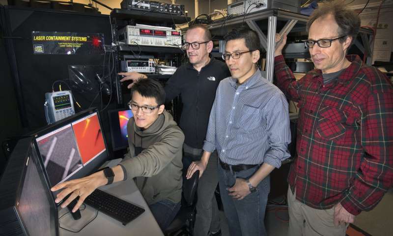
(Left
to right) Mingxing Li, Mircea Cotlet, Chang-Yong Nam, and Percy Zahl at the new
scanning photocurrent microscopy facility at Brookhaven Lab's Center for
Functional Nanomaterials. Photo courtesy of the Brookhaven National Laboratory.
Scientists at the Center for Functional Nanomaterials (CFN)"”a US Department of Energy (DOE) Office of Science User Facility at Brookhaven National Laboratory"”have used an optoelectronic imaging technique to study the electronic behavior of atomically thin nanomaterials exposed to light. According to the researchers, combining their nanoscale optical imaging techniques with scanning photocurrent microscopy becomes a powerful tool for understanding the processes affecting the generation of electrical current (photocurrent) in these materials. They believe that such an understanding is key to improving the performance of solar cells, optical sensors, light-emitting diodes (LEDs), and other optoelectronics that rely on light-matter interactions to convert light into electrical signals or vice versa.
"Anyone who wants to know how light-induced electrical current is distributed across a semiconductor will benefit from this capability," said CFN materials scientist Mircea Cotlet, co-corresponding author of a paper about the Brookhaven National Laboratory findings that appears in the 17 May edition of Advanced Functional Materials.
Generating an electrical current
When hit with light, semiconductors generate an electric current. Semiconductors that consist of one layer or a few layers of atoms"”for example, graphene, which has a single layer of carbon atoms"”are of particular interest for next-generation optoelectronics because of their sensitivity to light, which can controllably alter their electrical conductivity and mechanical flexibility. However, the amount of light that atomically thin semiconductors can absorb is limited, thus limiting the materials' response to light.
To enhance the light-harvesting properties of these two-dimensional (2-D) materials, scientists add tiny (10"“50 atoms in diameter) semiconducting particles called quantum dots in the layer(s). The resulting "hybrid" nanomaterials not only absorb more light but also have interactions occurring at the interface where the two components meet. Depending on their size and composition, the light-excited quantum dots will transfer either charge or energy to the 2-D material. Knowing how these two processes influence the photocurrent response of the hybrid material under different optical and electrical conditions"”such as the intensity of the incoming light and applied voltage"”is important to designing optoelectronic devices with properties tailored for particular applications.
"Photodetectors sense an extremely low level of light and convert that light into an electrical signal," explained Cotlet. "On the other hand, photovoltaic devices such as solar cells are made to absorb as much light as possible to produce an electrical current. In order to design a device that operates for photo detection or photovoltaic applications, we need to know which of the two processes"”charge or energy transfer"”is beneficial."
Further details of the group's findings can be found by visiting this link with the browser of your choice: https://phys.org/news/2018-05-light-induced-electrical-current-atomically-thin.html#jCp


