
Researchers Confine Light in a Single Atom
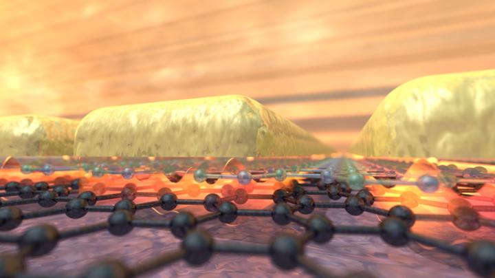
Artistic
impression of the squeezed light (plasmon) in between the metal and graphene,
separated by a one-atom-thick dielectric. Courtesy of ICFO.
Using graphene, researchers in Spain, Portugal and the US have found a way to confine light to a space that is one atom thick. The ability to confine light to such a small space could pave the way for ultra-small optoelectronic devices. Details of their work appear in the journal Science.
Previous work has shown that while metals can compress light below the diffraction limit, this additional confinement typically comes at the cost of additional energy loss. A team from Barcelona's Institute of Photonic Sciences (ICFO), the University of Minho in Portugal, and the Massachusetts Institute of Technology (USA) has addressed this issue by building a graphene-insulator-metal heterostructure that can overcome the trade-off between confinement and losses.
The researchers fabricated a nano-optical device from 2D heterostructures. They used a graphene monolayer, which acted as a semimetal, and stacked onto it a hexagonal boron nitride (hBN) monolayer, which served as an insulator. Graphene was used because it can guide light in the form of plasmons "” oscillations of electrons interacting with light.
On top of the graphene-hBN structure, researchers deposited an array of metallic rods.
Researchers sent IR light through the device and observed how plasmons in between the metal and the graphene propagated. They reduced the gap between the metal and the graphene to see if the confinement of light remained efficient, that is, it did not incur additional energy losses. Experiments showed that even when a single monolayer of hBN was used as a spacer, the plasmons were excited by the light and were able to propagate freely while being confined to a channel just on atom thick. The light was confined vertically (as propagating plasmons) between the metal and the graphene.
"At first we were looking for a new way to excite graphene plasmons. On the way, we found that the confinement was stronger than before and the additional losses minimal. So we decided to go to the one-atom limit with surprising results," said ICFO researcher David Alcaraz Iranzo.
Researchers were able to switch the plasmon propagation on and off by applying an electrical voltage. Using this capability they demonstrated the control of light guided in channels smaller than one nanometer.
This shift in optical field confinement could further the exploration of extreme light-matter interactions in ways not previously possible.
"Graphene keeps surprising us: nobody thought that confining light to the one-atom limit would be possible. It will open a completely new set of applications, such as optical communications and sensing at a scale below one nanometer," said ICFO professor Frank Koppens.
Such heterostructures could provide a powerful and versatile platform for nanophotonics. The atomic-scale "toolbox" of 2D materials could be used for devices where both photons and electrons would be controlled down to the nanoscale, and could lead to new devices, such as ultrasmall optical switches, detectors, and sensors.


