
Researchers See Promise in New Optical CMOS Process
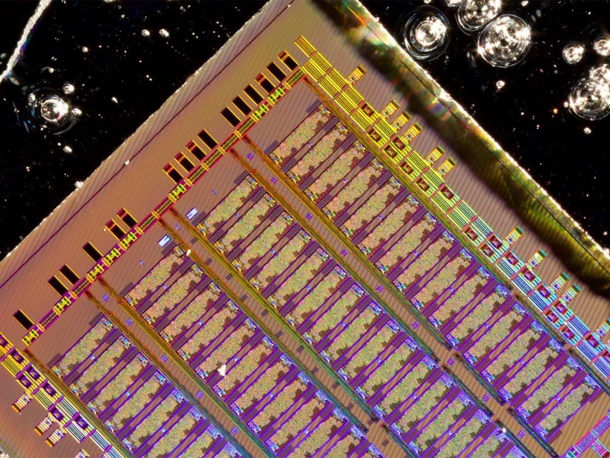
Photo by: Amir Atabaki
Researchers at five US-based universities and institutes have reported the development of a new optical CMOS process that they believe could speed the creation of photonic integrated circuits (PICs) and other related optical components. According to reports in "˜Nature' and "˜IEEE Spectrum,' the teams have added thin layers of polycrystalline silicon atop features patterned using existing CMOS technologies. They believe the process could speed the development of faster photonic circuits benefiting many datacom and telecom applications.
"What we're talking about is integrating optics with electronics on the same chip," says Milos Popovic, a professor of electrical and computer engineering at Boston University. The method entails adding "a handful" of processing steps to the standard way of making microprocessors in bulk silicon and should not add much time or cost to the manufacturing process, Popovic says.
Popovic worked on the development at Boston University together with teams at the Massachusetts Institute of Technology; the University of California, Berkeley; the University of Colorado, Boulder; and SUNY Polytechnic Institute, Albany, NY. Their approach adds a thin layer of polycrystalline silicon on top of features already on the chips. The same material is used on chips as a gate dielectric, but in a form that absorbs too much light to be useful as a waveguide.
Researchers explained that to make a material more suitable for photonics, they adjusted the deposition process, altering factors such as temperature, to obtain a different crystalline structure. They also took trenches of silicon dioxide, already used to electrically isolate transistors from one another, and made them deeper, to prevent light from leaking out of polycrystalline silicon features into the silicon substrate.
Using the approach, teams built chips with all the necessary photonic components"”waveguides, microring resonators, vertical grating couplers, high-speed modulators, and avalanche photodetectors"”along with transistors with 65-nm feature sizes. In this scenario, a laser light source would sit outside the chip. The photodetectors rely on defects that absorb the photons. The chips were built at the 65 nm node because that is what the semiconductor manufacturing research fab at SUNY Albany is capable of, but Popovic says it should be easy to apply the same processes to transistors being made with much smaller features.
Many of the same researchers had come up with a process for integrating photonics on chips in 2015, but that only worked on more expensive silicon-on-insulator processors. The vast majority of chips are made using bulk complementary metal-oxide-semiconductor technology, which this new technique addresses.
The reason this is all necessary is that computer makers are increasingly relying on multicore chips; graphical processing units used for gaming and artificial intelligence can contain hundreds of cores. The copper wires that carry data between cores are the major bottleneck for speed, as well as producing a lot of waste heat.
"A single electrical wire can only carry 10 to 100 gigabits per second, and there's only so many you can put in," Popovic says. By contrast, splitting the signal into many wavelengths could allow a single optical fiber to carry 10 to 20 terabits per second. And at the tiny distances between microprocessors, optical losses are basically zero, so the system requires less power than copper.
This new method could lead to chips with increased processing power that would allow greater use of artificial intelligence techniques for pattern recognition. That could bring the facial recognition used in iPhones to less expensive smartphones, Popovic says, as well as create low-cost LIDAR sensors for self-driving cars.


