
New Approach for Stabilizing Optical Nanocrystals
KAUST researchers have announced new findings that point to improved surface passivation of perovskite nanocrystals through the use of IDA molecules for greater stability as well as improved optical and electrical properties, making them potentially more useful for optoelectronic devices.
- A method for chemically stabilizing optical nanocrystals without degrading their electrical properties has been developed by scientists at the King Abdullah University (KAUST) in Saudi Arabia.
The researchers said that they believe halide perovskites are in an exciting class of materials for optoelectronics and photovoltaics. These materials efficiently absorb visible light, possess long charge-carrier diffusion lengths and are easy and cheap to produce. The performance of optical devices can also be improved by incorporating nanometer-scale particles, which have far superior light emitting and absorbing properties compared to the bulk material from which they are derived. So it is unsurprising that scientists are keen to combine these two approaches. The challenge is that tiny perovskite particles aren't always chemically stable, and their atomic crystal structure is difficult to control, not to mention the fact that many perovskite chemistries contain lead or cadmium, resulting in manufacturing, usage and disposal complications.
Attaching molecules, referred to as ligands, can stabilize a nanocrystal, they noted. But this so-called passivation can form an electrically insulating shell around the particle that inhibits their effectiveness in electronic devices.
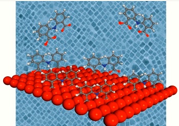
Now, Osman Bakr's group, and co-workers from KAUST and ShanghaiTech University, have created halide perovskite nanocrystals made from cesium-lead-iodide passivated by 2,2"²-iminodibenzoic acid (IDA) ligands. They show that this provides the necessary chemical stability while remaining useful for optoelectronics. And the passivation was simple: just adding IDA powder into the nanocrystal solution and using a centrifuge to remove any excess.
The team chose IDA because it is a bidentate ligand, meaning that it bonds to the nanocrystal at two sites. "The conventional ligands used in these applications, such as oleic acid, are dynamic on the surface of the perovskite nanocrystals and easily come loose," says Jun Pan, the first author on the paper. "That's why we apply a double carboxylic group to strongly bind on the surface, which also stabilizes the perovskite crystal phase at room temperature."
Pan and his team compared the optical properties of both the passivated and unpassivated samples and observed that the treatment improved the photoluminescent quantum yield"”a measure of how many photons are emitted for every photon absorbed"”from 80 percent to over 95 percent. And while the intensity of light emitted from the unpassivated nanocrystals had dropped significantly five days later, the IDA-treated samples were still emitting light at 90 percent of their initial level 15 days later.
Passivating the surface of perovskite nanocrystals with IDA molecules improves their stability and their optical and electrical properties, making them useful for optoelectronic devices.
The team demonstrated that their stabilized halide perovskite nanocrystals were suitable for optoelectronic applications by using them to build light-emitting diodes. The red-light generating devices again outperformed the unpassivated control device in terms of maximum luminance and luminous power efficiency.
"The next step is to realize more stable perovskite structures and to create an LED with performance above 10 percent based on perovskite nanocrystals," says Pan.


