
Ayar Labs' PIC Tech Moves Towards Release
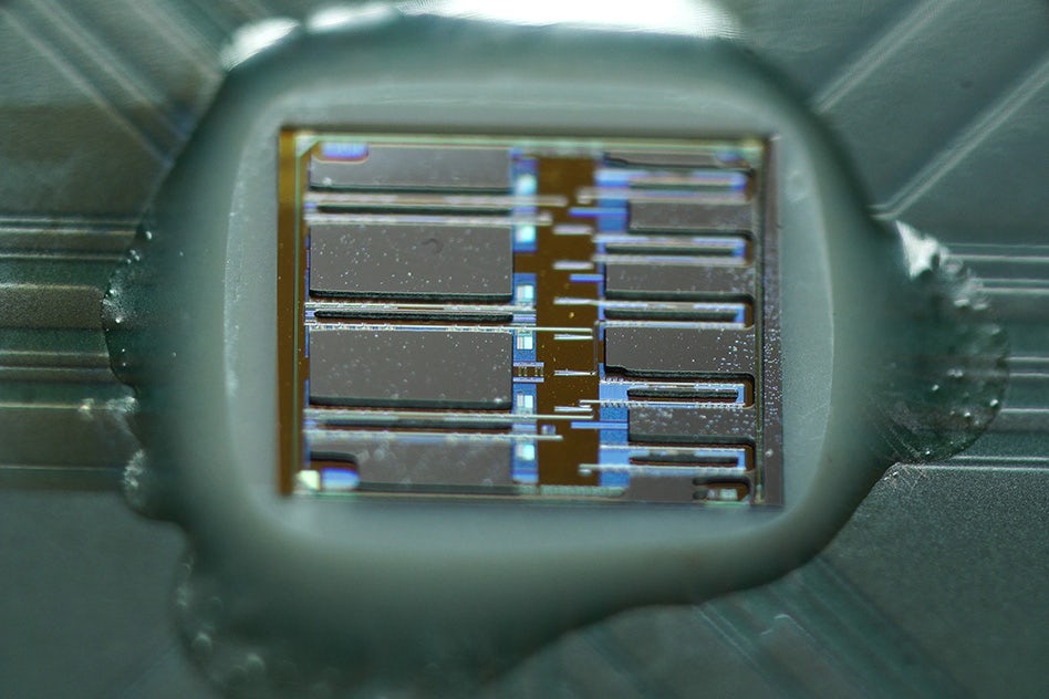
Image of prototype PIC device courtesy of Ayar Labs and MIT.
In an article from the Massachusetts Institute of Technology (MIT) the university commended Ayar Labs as it moves towards the release of its new photonic integrated circuit (PIC) design that is set to reduce energy consumption in chip-to-chip communications by up to 95 percent while potentially cutting energy utilization at major data centers as much as 50 percent.
Ayar Labs was recently honored at PIC International with a 2018 Advances in Photonic Integration Award after the new company penned a deal with GlobalFoundries in late 2017 to support further development. A 2019 product release is expected. Accepting the PIC International award was Mark Wade, Ayar Lab's co-founder, president and chief scientist.
In an article by the MIT News Office, the university notes that since the invention of the silicon chip 60 years ago, the power of computers doubled every two years as described by Intel co-founder Gordon Moore in his now famous 'Moore's Law' predictor of chip evolution. But the speed at which computer systems work hasn't shown quite such dramatic progress. The problem is one of data transmission and the bottlenecks that any technology runs into--its slowest component drags down overall performance.
Think of a computer as like an air passenger system. If you concentrate on the aircraft, airport runway architecture, supply logistics, and air traffic control, it's easy to speed up travel between, for example, New York and Washington DC to under one hour. That sounds fantastic, but if it takes you two hours to get through security at one hand and another two hours to collect your baggage at the other, then it's faster to drive.
It's the same with computers. Chips may be able to operate at lightning speed, but most still communicate with one another using copper wires that not only slow down the system, they also force the chips to waste energy sitting idle while the data is transferred. As long as the copper wires are there, so is the bottleneck.
One way of handling this problem is to create a computer that uses light instead of electricity. Such photonic chips take up little space, work literally at the speed of light, can send multiple signals at once on various wavelengths, and are very energy efficient "“ but their development, despite decades of research, is still far behind that of their electron-based cousins.
The Ayar Labs solution to this conundrum is to create a hybrid chip that melds optical and electronic elements. This isn't new, but where previous attempts wasted energy by treating the photonic and electronic parts as separate elements, Ayar cut out the copper to create silicon chips that directly integrate optical components at a cost of pennies per chip.
In December, Ayar Labs reached a deal with top silicon chip manufacturer GlobalFoundries to bring its first product, an optical input-output system called Brilliant, to market next year.
The chips could also be used in supercomputers, says Ayar Labs CEO Alex Wright-Gladstein, noting that supercomputers have similar efficiency issues and speed constraints as data centers. Down the road, the technology could also improve optics in various fields, from autonomous vehicles and medical devices to augmented reality. "We're excited about not just what this can do for data centers, but what new things this will enable in the future," Wright-Gladstein says.
Seeing the light
Ayar's core technology "” now backed by more than 25 academic papers "” has been a decade in the making. The research collaboration began in the mid-2000s at MIT as part of the Defense Advanced Research Project Agency's Photonically Optimized Embedded Microprocessors (POEM) project, led by Vladimir Stojanovic, now an associate professor of electrical engineering and computer science at the University of California at Berkeley, in collaboration with Rajeev Ram, an MIT professor of electrical engineering and principal investigator for the Physical Optics and Electronics group, and Milos Popovic, now an assistant professor of electrical and computer engineering at Boston University.
The idea was to help data transmission keep up with Moore's Law. The number of transistors on a chip may double every two years, Wright-Gladstein says, "but the amount of data we push across those copper pins hasn't grown at the same rate."
Computer chips send data between chips with different functions, such as logic chips and memory chips. With copper-based communications; however, the chips can't send and receive enough data to take advantage of their increasing processing power. That's caused a "bottleneck," where chips must wait relatively long durations to send and receive data. More than half the time in data centers, for instance, circuits are waiting for data to come and go, Wright-Gladstein says. "It's a huge waste," she says. "They're using almost as much power idling as when they are working."
One solution is light. An optical wire can transmit multiple data signals on different wavelengths of light, while copper wires are limited to one signal per wire. Optical chips can, therefore, transmit more information using significantly less space. Moreover, photonics produce very little waste heat. Data passing through copper wires generates large amounts of waste heat, which hurts efficiency in individual chips. This is an issue in data centers, where copper wires run inside and between servers.
At the time that the research groups of Ram, Stojanovic, and Popovic were working on the POEM project, large companies such as Intel and IBM were trying to design inexpensive, scalable optical chips. The collaboration "” which then included Sun and Wade "” took a different approach: They integrated optical components onto silicon chips, which are fabricated using the traditional CMOS semiconductor manufacturing process that churns out chips for pennies. "That was radical idea at time," Wright-Gladstein says. "CMOS doesn't lend itself well to optics, so industry veterans assumed you'd have to make major changes to get it to work."
To avoid making changes to the CMOS process, the researchers focused on a new class of miniaturized optical components, including photodetectors, light modulators, waveguides, and optical filters that encode data on different wavelengths of light, and then transmit and decode it. They essentially "hacked" the traditional method for silicon chip design, using layers intended for electronics to build optical devices, and enabling chip designs to include optics more tightly configured than ever inside a chip's structure.
In 2015, the researchers, together with Krste Asanovic's team at UC Berkeley made the first processor to communicate using light and published the results in Nature. The chips, manufactured at a GlobalFoundries fabrication facility, contained 850 optical components and 70 million transistors, and performed as well as traditional chips manufactured at the same facility.
Taking the plunge
Wright-Gladstein was already thinking about commercialization behind the scenes, and formed a team in her MBA class to create a business plan and pitch deck. She also collaborated frequently with Sun and Wade in speaking with potential industry clients. When the MIT Clean Energy Prize rolled around, the three students entered the technology under the name, OptiBit "” and won both grand prizes for $275,000, solidifying their decision to launch a startup.
"Having funds early on to pay ourselves low salaries and having a little cushion before raising venture capital funds really persuaded us all to take the plunge," Wright-Gladstein says.
Setting up shop in San Francisco, the startup continued research and development, increasing the communication data rates of the technology. Last year, GlobalFoundries took interest in these constant innovations and struck a partnership with the startup, which included some undisclosed funding. This year, Ayar's first prototypes should reach U.S. data centers, with a planned 2019 commercial release.
Solving the chip input-output problem is just the start. Ayar is also excited about what its new technology means for the field of optics, Wright-Gladstein says. Optical sensors, for instance, are used in self-driving or semiautonomous vehicles and expensive medical equipment. Lowering manufacturing costs, while increasing the computation power, of optoelectronic chips could make those technologies much less expensive and more accessible.
"We're starting out solving this bottleneck problem in traditional silicon chips, but ultimately we're excited about all the different places this technology will go," Wright-Gladstein says. "This is going to change the availability of optics, and how the world can use optics, in ways beyond what we can predict right now."


