Leti Offers New PIC Design Kit with Synopsys

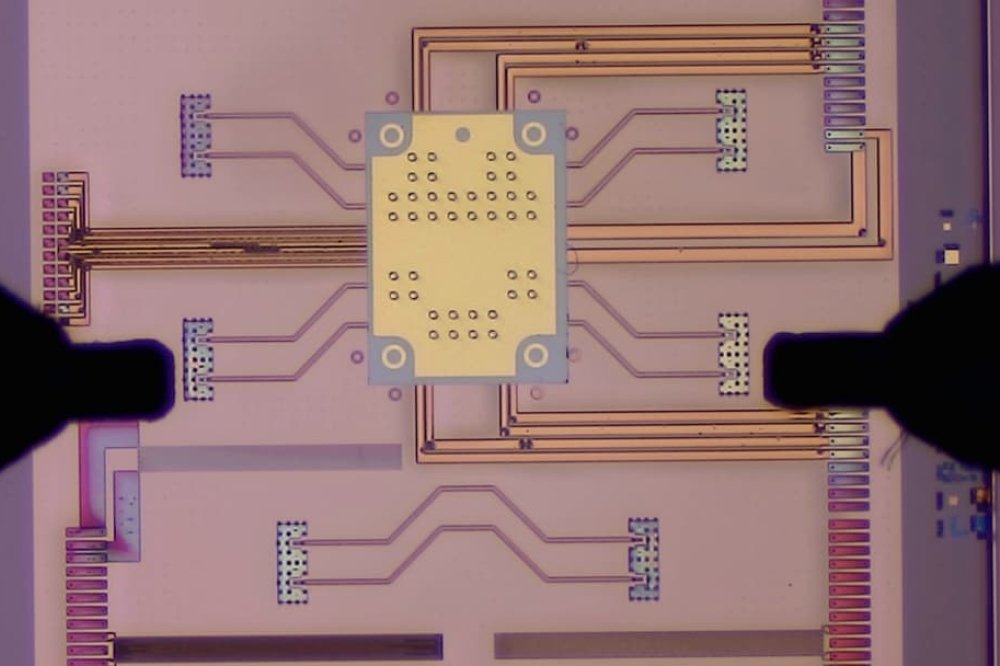
Leti has announced that a new photonics process design kit (PDK) for photonic circuits is available in the Synopsys PhoeniX OptoDesigner suite. The kit contains design rules and building blocks for multi-project wafer (MPW) and custom runs on Leti's Si310 Platform.
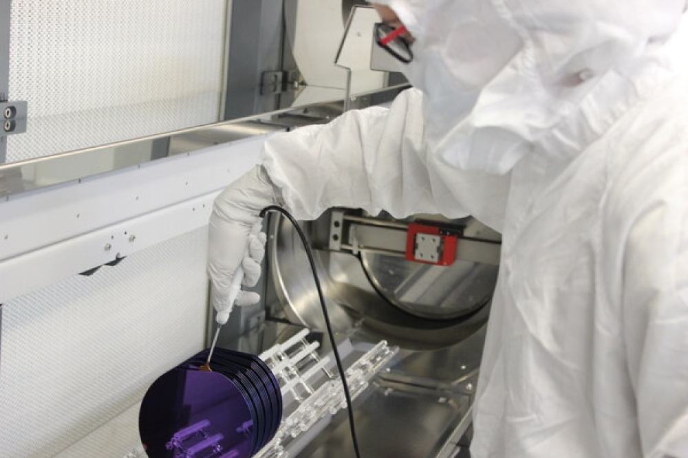
According to CEA-Leti (Grenoble, France) its integrated silicon photonics platform has been developed for high-speed optical transceivers and highly-integrated optical interposer applications. In addition to design rules and building blocks it also includes a catalogue of components available at Leti, allowing Synopsys PhoeniX OptoDesigner customers to select elements they need to build their circuits. Once customers have a completed circuit design, Leti produces a proof of concept on a multi-project wafer run.
Synopsys PhoeniX will present a two-day workshop exploring electro-photonic design automation (EPDA) for photonic integrated circuits (PICs) at the PIC International Conference, 10-11 April at the Sheraton Brussels Airport Hotel. Delegates will learn how to use the latest software automation and optimization techniques for photonic circuit design, simulation and fabrication including OptoDesigner and other major elements of its EPDA tool catalogue. For more information or to register, please visit the PIC International Training website: http://training.picinternational.net/
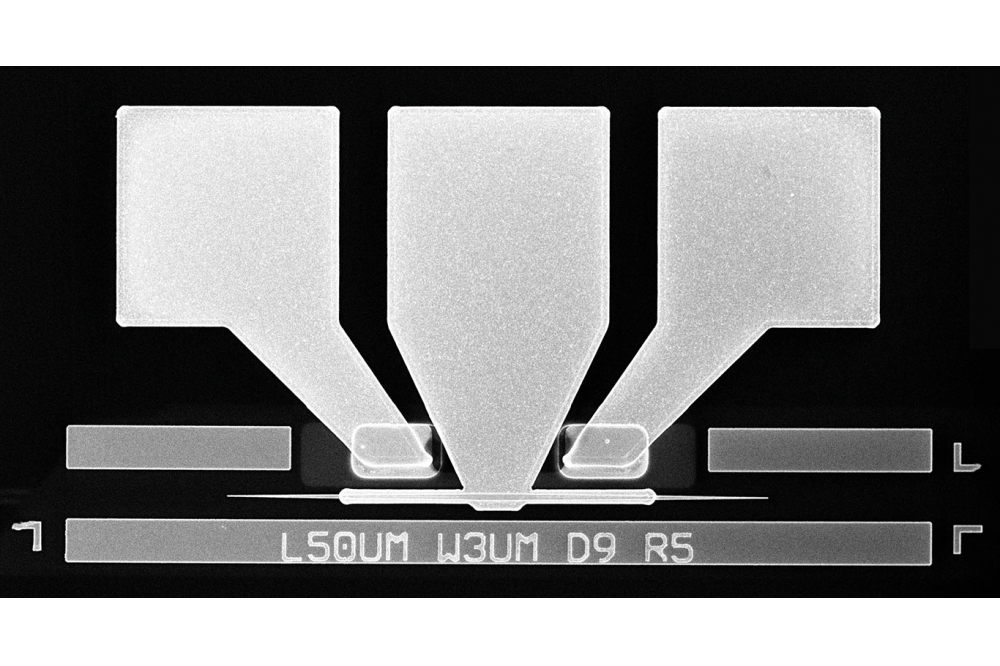
Used by more than 300 designers worldwide, OptoDesigner gives access to a complete set of passive components, such as grating couplers, silicon waveguides and transitions; and active components, such as high-speed Mach Zehnder modulators and high-speed germanium photodiodes based on Leti's fab. The PDK also includes physical verification tools for checking whether contributions meet the design rules defined by Leti's clean room fabrication constraints.
"On the same mask, with this design kit, we are able to have photonic circuits performing various functions, according to the area of expertise of the different contributors," said Andre Myko, responsible of MPW runs at Leti. "Fabless companies and academics therefore can realize substantial cost savings by "˜sharing' production costs on multi-project wafer runs."
Leti is a world leader in silicon photonics technology. Its photonic platform is France's largest R&D center for the development, characterization and simulation of optoelectronic systems and components. Its activities range from component design through component fabrication, integration into systems and packaging.
"Leti's process design kit available for Synopsys' PhoeniX OptoDesigner is a licensed plug-in library of solutions that support multi-project wafers and custom runs provided by Leti," said Niek Nijenhuis, global business development manager of Synopsys' PhoeniX OptoDesigner products. "In addition to the photonic elements from the standard OptoDesigner library, Leti's PDK contains technology-specific information like mask layer names, design rules, validated building blocks, die sizes and GDS file settings."
Leti's silicon photonics platform is also fully compatible with STMicroelectronics' platform in Crolles, which enables fabless customers to take their new circuits to high-volume production.


