Opportunities Drive Soitec's Silicon Photonics Focus
The researchers of Yole Développement (France) met recently with Soitec's VP of digital electronics to discuss the company's production capacity to meet existing and future silicon photonic (SiP) growth projections. Highlights from the mid-March 2018 interview point to strong opportunities for incumbent manufacturers. At the same time, Yole and Soitec see good opportunities for new entrants thanks to the market's overall short- and long-term potential.
SiP and photonic integrated circuit (PIC) markets continue to attract interest from companies large and small due to the world's seemingly endless appetite for more high speed data transport. While major data center companies including Google, Amazon and Facebook along with global manufacturers are driving standards, the entire market has substantial potential, with projections of 25 percent compound annual growth rates (CAGR) or higher regularly cited.
According to Yole, silicon photonics is still a relatively small market, with sales at die level estimated to be (USD) $30 million in 2016. However, it has "˜big promise,' with a 2025 market value of $560 million at chip level and almost $4 billion at transceiver level. This development path means that silicon photonics technology will grow from a few percent of the total optical transceiver market value in 2016 to 35 percent of the market in 2025, mostly for intra-data center communication, the researchers state.
Yole stated that it sees the strongest SiP demand at present is for new 400G solutions, which was born out in product releases, paper presentations and keynote addresses from OFC 2018 that concluded recently in San Diego, California. Yole researchers see 200G devices/applications as possibly an intermediate step between 100G and 400G. The next evolutionary benchmark is to develop a 400G optical port over a single fiber across 500m at less than $1 per gigabit and with power <5mW/Gb. One terabit per second (T/bps) rates should follow, they believe. Although the wafer area this accounts for will be a minute part of the worldwide silicon-on-insulator (SOI) market, it will represent significant value because of SOI wafer prices; the main SOI supplier is SOITEC, according to Yole.
Dr. Eric Mounier, Senior Analyst in Silicon Photonics at Yole Développement, sat down with Christophe Maleville, Executive Vice President for the Digital Electronics Business Unit at Soitec, a major supplier of SOI wafers for silicon photonics, to discuss their vision of the market and for this exciting technology. Excerpts and highlights of the interview follow; visit Yole Developpement for complete details at: https://www.i-micronews.com/photonics-expertise/10968-soitec-is-ready-to-serve-large-volume-silicon-photonics-markets.html?utm_source=@micronews&utm_medium=email&utm_campaign=@MN_Mar162018
Eric Mounier: Can you describe Soitec's involvement in silicon photonics?
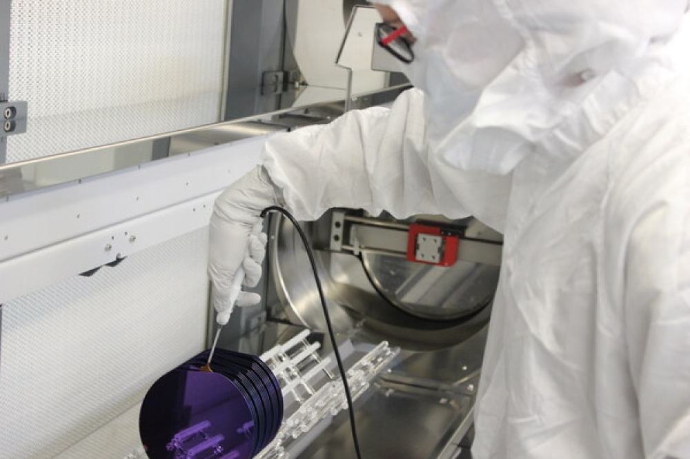
Christophe Maleville: The best and most natural way to manufacture silicon photonics chips and devices is to use silicon-on-insulator (SOI) wafers because they integrate the vertical structures of optical waveguides "¦ Our photonics SOI wafers provide a platform for integrating high-quality photonics functionalities and silicon-based devices while also allowing the use of standard manufacturing processes.
EM: What are SOI wafers' key parameters for silicon photonics?
CM: The key parameters required by the industry are silicon thickness uniformity and surface roughness. Our Photonics-SOI wafers have a silicon thickness in the range of 100 nm to 500 nm and the thickness of the buried-oxide layer is in the range of 1 µm to 3 µm. These wafers' surface roughness is comparable to bulk silicon wafers. We provide both 200 mm and 300 mm wafer diameters.
EM: Can you comment on Soitec's products' added value for silicon photonics chips?
CM: Soitec has been developing SOI technology solutions to meet silicon photonics' requirements for more than a decade. Soitec's best-in-class 200 mm and 300 mm photonics-SOI wafers have top-silicon uniformity of +/-3 nm on all wafers with a roadmap to reach +/-1 nm. Soitec also has the largest SOI manufacturing capacity in both 200-mm and 300-mm diameter wafers.
EM: What is Soitec's production capacity for silicon photonics?
CM: Soitec has multiple fabs manufacturing SOI products designated for different markets (including) photonics SOI products; manufacturing capacity is over one million wafers.
EM: What do you see as the next applications driving silicon photonics markets?
CM: Today, the primary application driving silicon photonics' production volume is high-speed Ethernet interconnections for data centers and high-performance computing (HPC). Silicon photonics' market penetration will increase with the evolution of 100G, 400G and 800G standards. We also expect to see the integration of optical interconnection directly on application-specific integrated circuits (ASICs) such as switch ASICs and CPUs within the next five years "¦ Metro Ethernet and especially 5G backhaul are also emerging applications "¦ Silicon photonics also will become a key element of fully autonomous cars, in which ultra-high-speed connectivity between different sensors and computing units will be absolutely essential.
EM: The silicon photonics market is currently in the hands of a few companies, mainly Intel and Luxtera, but many startups are emerging. How do you foresee the evolution of the industrial landscape in the coming years?
CM: (While) it's true that Intel, Luxtera and Cisco were the first to bring the vision on silicon photonics to the market, the ecosystem is very big. It is populated by startups, research centers and major industrial players at all levels of the data center value chain including photonics components makers, server manufacturers, data center providers, companies offering cloud computing services and major consumer companies. Now that demand is increasing, large foundries are entering, aiming to offer a generic production process to their fabless customers. In the coming years, we will probably see some standardization of silicon photonics production by each foundry. At that point, fabless companies will differentiate their products through designs and applications.
EM: Do you see the involvement of large IC foundries such as TSMC in silicon photonics as an encouraging sign for this technology?
CM: Today few major foundries offer services based on photonics SOI. Publically, GlobalFoundries, TowerJazz and TSMC are active in the market. Some others are getting ready to bring their offerings to market ... Silicon photonics is ready to serve large-volume markets.


