GCS, Intengent, VLC to offer PIC Fab Services

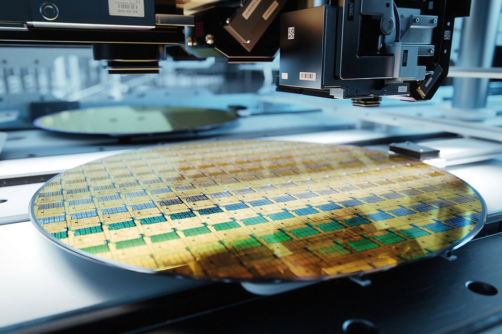
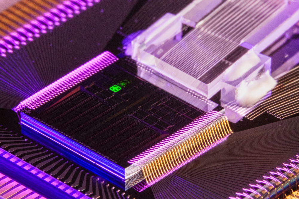
Semiconductor wafer fabrication foundry Global Communication Semiconductors LLC, III-VI photonic consultant Intengent and photonic integrated circuit designer VLC Photonics SL will jointly offer fabless development into production services for customised photonic integrated circuits (PICs) in indium phosphide (InP).
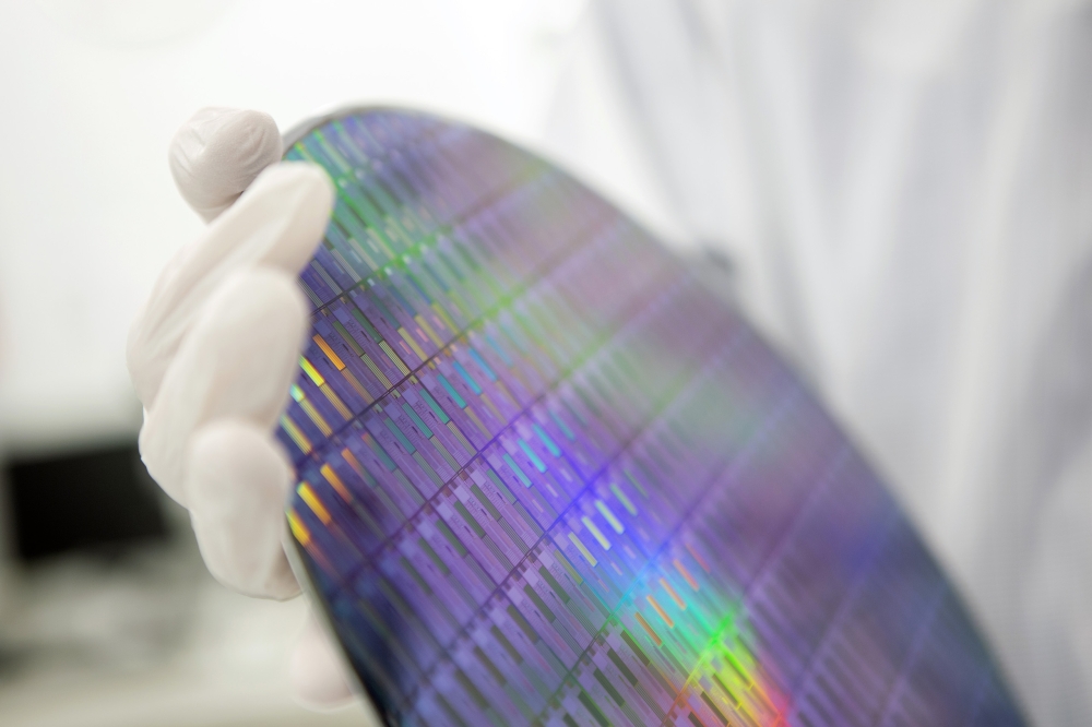
GCS provides a broad range of wafer foundry services based on a proprietary regrowth-free InP process. Originally developed as a state-of-the-art opto and heterojunction-bipolar-transistor (HBT) processes, it also allows for prototyping and volume-scalable production of PICs. The key enabler is a photonic integration platform that is compatible with the foundry's regrowth-free process and yet suitable for a variety of applications.
"Our well-established processes have great synergies with the TAVI PIC platform," said Brian Ann, CEO of GCS. "Our 4,6 inch wafer capability, based on a commercially supplied one-step-growth epitaxy, creates a unique opportunity for InP PICs. We believe that the GCS"“Intengent"“VLC partnership can fully utilize this opportunity and generate significant PIC business in various markets. By leveraging the infrastructure and expertise that we have gained in high-volume RF and optoelectronics markets, this partnership offers time/cost-efficient PIC development into production."
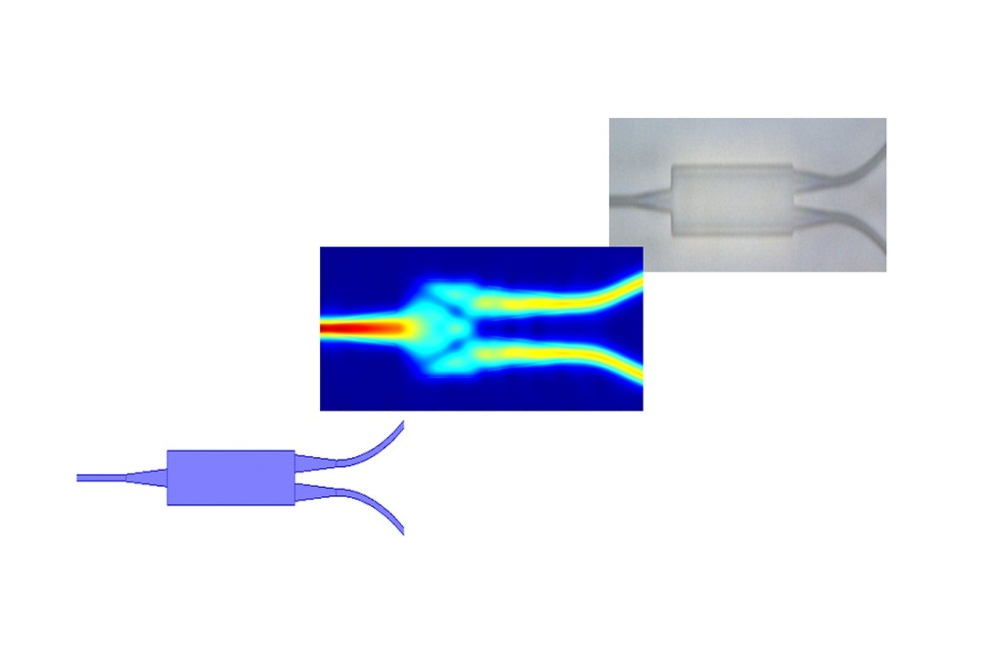
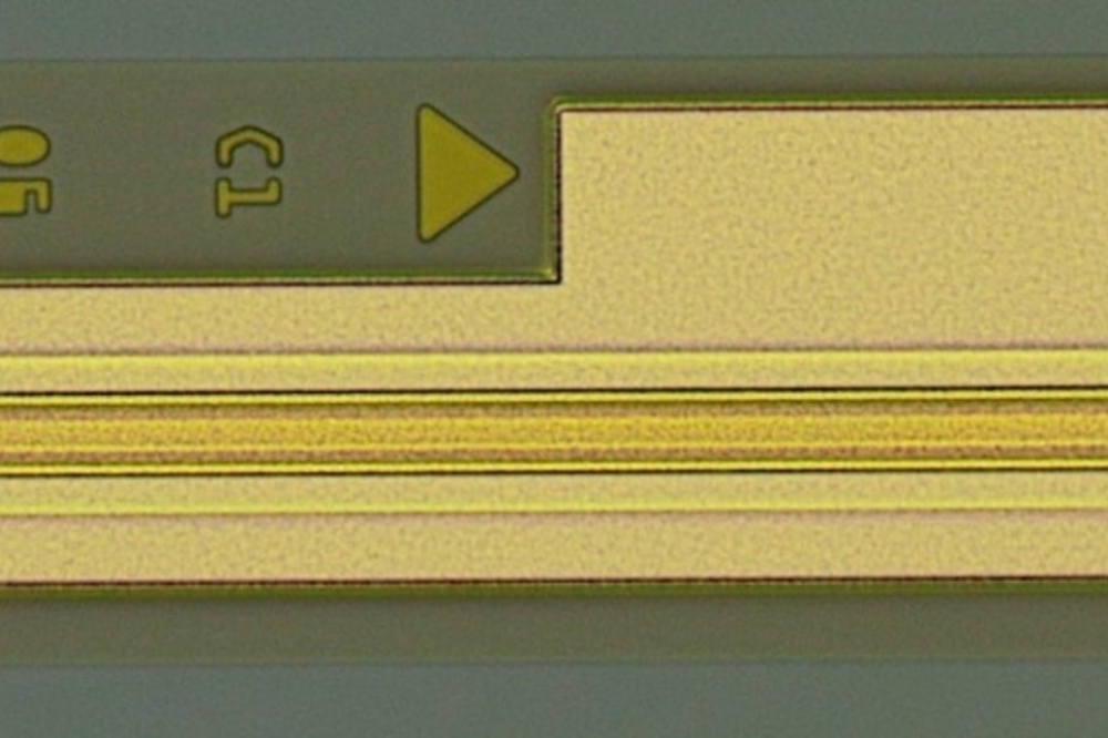
Intengent has developed Taper Assisted Vertical Integration (TAVI), which is regrowth-free and based on the GCS process, enabling decoupling of epitaxial growth and wafer fabrication. TAVI covers many PIC applications, including those in growing and emerging markets such as optical interconnects and switching markets. It also offers complimentary solutions to silicon photonics.
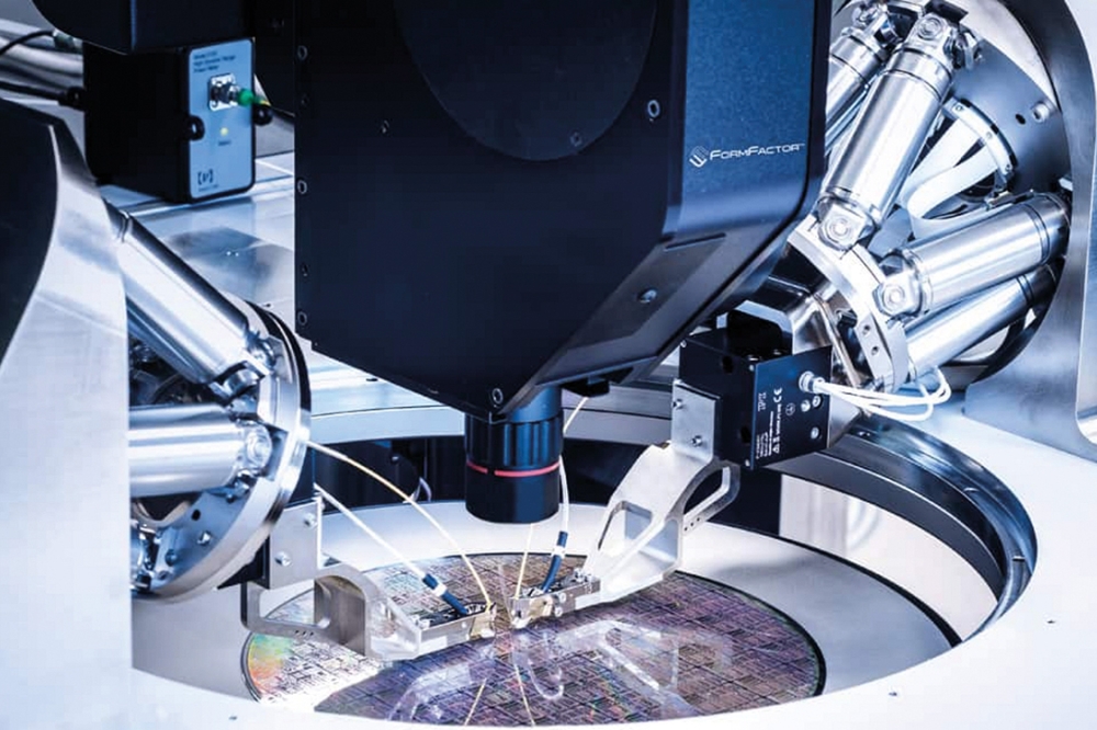
"GCS is an advanced III-V foundry with a high InP wafer throughout both in [radio frequency] electronics and optoelectronics markets," said Valery Tolstikhin, CEO of Intengent. "The TAVI platform takes advantage of GCS' process maturity and extends it to PICs in InP. To make the technology suitable for a fabless PIC development, one more thing is needed: the PDK. This is where VLC comes in, bringing a wealth of experience in PIC design and characterization. The fabrication process, the integration platform and the PDK together make a versatile generic platform for PICs in InP that allows the end users to access the commercial-grade technology under the fabless model."


