Ultra-thin metalens brings colour into focus
University of Washington team shows a new way to make tiny, next-generation imaging systems
In a paper published Feb. 9 in Science Advances, scientists at the University of Washington have described a way to successfully combine two different imaging methods - a type of lens designed for nanoscale interaction with lightwaves, along with robust computational processing - to create full-colour images.
The team's ultrathin lens is part of a class of engineered objects known as metasurfaces. Metasurfaces are 2D analogues of metamaterials, which are manufactured materials with physical and chemical properties not normally found in nature.
A metalens consists of flat microscopically patterned material surfaces designed to interact with lightwaves. To date, images taken with metalenses yield clear images - at best - for only small slices of the visual spectrum. But the UW team's metalens - in conjunction with computational filtering - yields full-colour images with very low levels of aberrations across the visual spectrum.
"Our approach combines the best aspects of metalenses with computational imaging - enabling us, for the first time, to produce full-colour images with high efficiency," said senior author Arka Majumdar, a UW assistant professor of physics and electrical engineering.
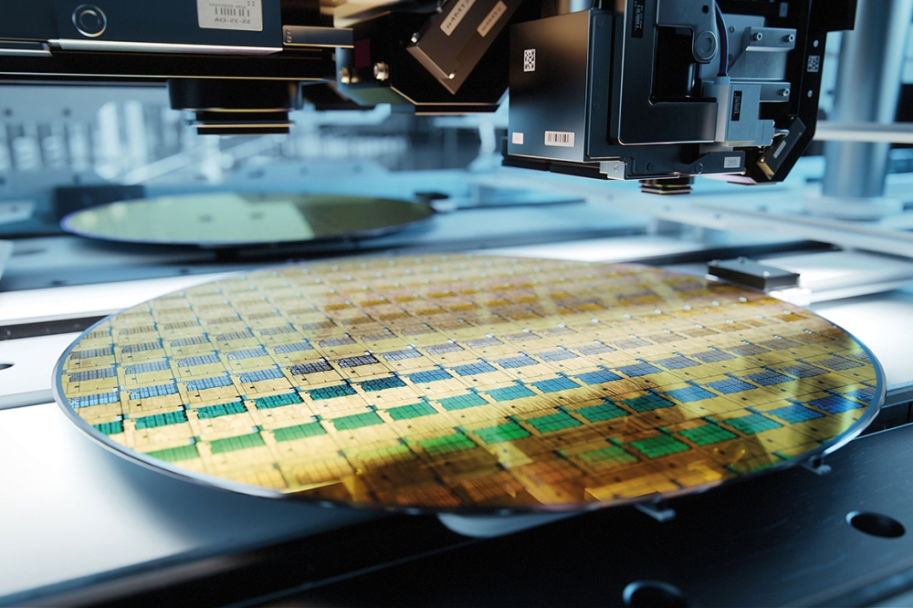
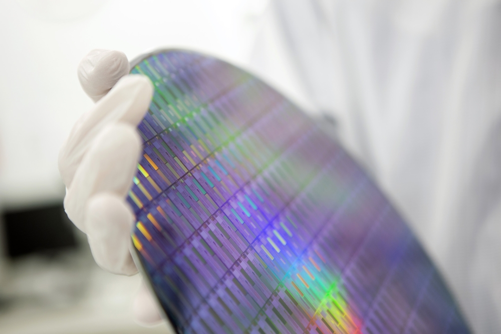
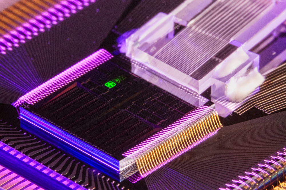
Instead of manufactured glass or silicone, metalenses consist of repeated arrays of nanometer-scale structures, such as columns or fins. If properly laid out at these minuscule scales, these structures can interact with individual lightwaves with precision that traditional lenses cannot. Since metalenses are also so small and thin, they take up much less room than the bulky lenses of cameras and high-resolution microscopes. Metalenses are manufactured by the same type of semiconductor fabrication process that is used to make computer chips.
"Metalenses are potentially valuable tools in optical imaging since they can be designed and constructed to perform well for a given wavelength of light," said lead author Shane Colburn, a UW doctoral student in electrical engineering. "But that has also been their drawback: Each type of metalens only works best within a narrow wavelength range."
In experiments producing images with metalenses, the optimal wavelength range so far has been very narrow: at best around 60 nanometers wide with high efficiency. But the visual spectrum is 300 nanometers wide.
Today's metalenses typically produce accurate images within their narrow optimal range - such as an all-green image or an all-red image. For scenes that include colours outside of that optimal range, the images appear blurry, with poor resolution and other defects known as "chromatic aberrations." For a rose in a blue vase, a red-optimised metalens might pick up the rose's red petals with few aberrations, but the green stem and blue vase would be unresolved blotches - with high levels of chromatic aberrations.
Majumdar and his team hypothesised that, if a single metalens could produce a consistent type of visual aberration in an image across all visible wavelengths, then they could resolve the aberrations for all wavelengths afterward using computational filtering algorithms. For the rose in the blue vase, this type of metalens would capture an image of the red rose, blue vase and green stem all with similar types of chromatic aberrations, which could be tackled later using computational filtering.
They engineered and constructed a metalens whose surface was covered by tiny, nanometers-wide columns of silicon nitride. These columns were small enough to diffract light across the entire visual spectrum, which encompasses wavelengths ranging from 400 to 700 nanometers.
Critically, the researchers designed the arrangement and size of the silicon nitride columns in the metalens so that it would exhibit a "spectrally invariant point spread function." Essentially, this feature ensures that - for the entire visual spectrum - the image would contain aberrations that can be described by the same type of mathematical formula. Since this formula would be the same regardless of the wavelength of light, the researchers could apply the same type of computational processing to "correct" the aberrations.
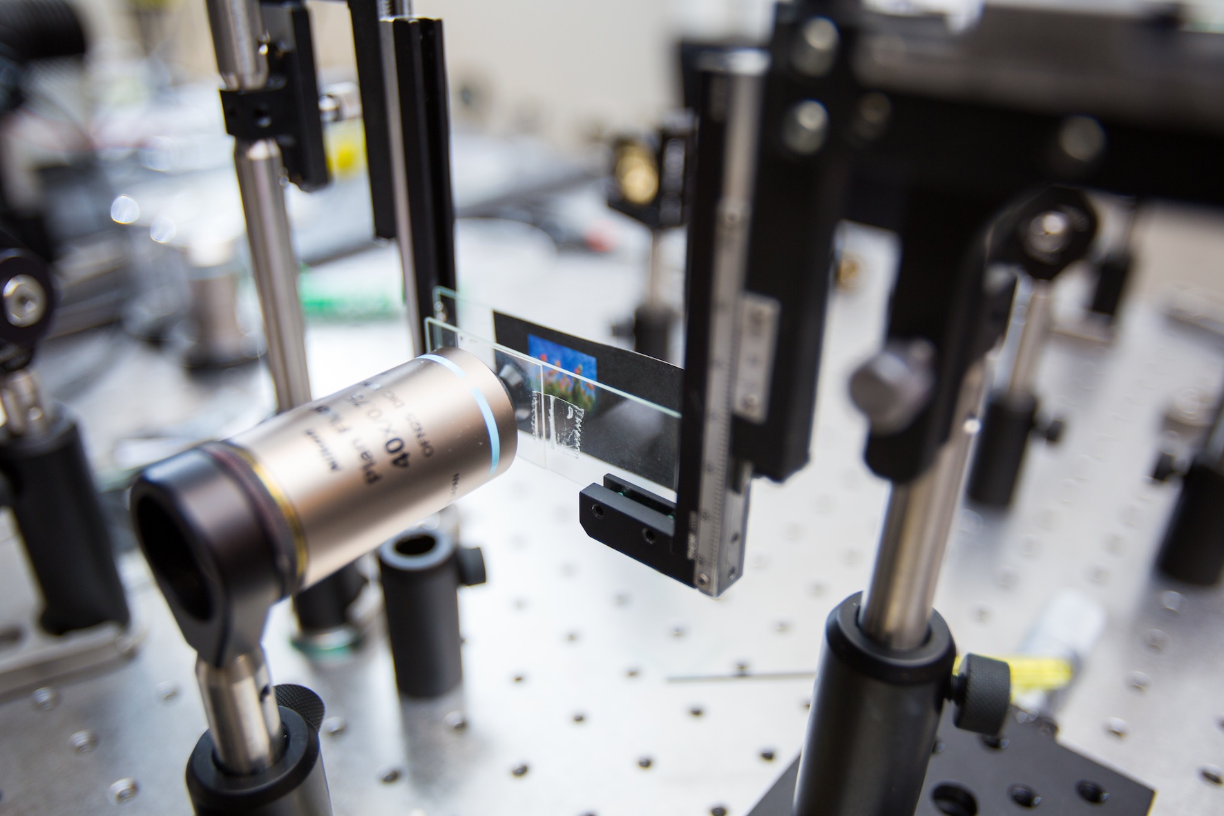
They then built a prototype metalens based on their design and tested how well the metalens performed when coupled with computational processing. One standard measure of image quality is 'structural similarity' - a metric that describes how well two images of the same scene share luminosity, structure and contrast. The higher the chromatic aberrations in one image, the lower the structural similarity it will have with the other image. The UW team found that when they used a conventional metalens, they achieved a structural similarity of 74.8 percent when comparing red and blue images of the same pattern; however, when using their new metalens design and computational processing, the structural similarity rose to 95.6 percent. Yet the total thickness of their imaging system is 200 micrometers, which is about 2,000 times thinner than current cellphone cameras.
"This is a substantial improvement in metalens performance for full-colour imaging - particularly for eliminating chromatic aberrations," said co-author Alan Zhan, a UW doctoral student in physics.
In addition, unlike many other metasurface-based imaging systems, the UW team's approach isn't affected by the polarisation state of light - which refers to the orientation of the electric field in the 3-D space that lightwaves are traveling in.
The team said that its method should serve as a road map toward making a metalens - and designing additional computational processing steps - that can capture light more effectively, as well as sharpen contrast and improve resolution. That may bring tiny, next-generation imaging systems within reach.
The research was funded by the UW, an Intel Early Career Faculty Award and an Amazon Catalyst Award.


