
Nanobulb can illuminate sub-wavelength size objects
ITMO scientists show how a silicon-gold nanoparticle can act as an effective source of white light when agitated by a pulse laser in IR band
Scientists from ITMO University, in St Petersburg, Russia, have proven that a silicon-gold nanoparticle can act as an effective source of white light when agitated by a pulse laser in IR band. One such 'nanobulb' was integrated into a standard probe microscope, which allowed the researchers to overcome the diffraction limit and examine subwavelength-size objects. The new technology makes modern near-field microscopy cheaper and simpler, also being potentially useful in medicine. The study has been published in Nano Letters.
In order to examine an object using a regular optical microscope, visual light is focused using special lenses. However, if the object is less than a wavelength in size, it cannot be observed in detail. This is what is called the diffraction limit.
There are several technologies today capable of overcoming this limit - for instance, near-field optical microscopy. In that case, the electromagnetic field of the object is measured in near field by using a special probe that can interact with the localised electromagnetic field and disperse it into the area where it can be registered by common detectors. Yet to get information about an object with a subwavelength resolution in a broad spectrum; researchers often spend hours scanning at different wavelengths until they cover the whole spectrum.
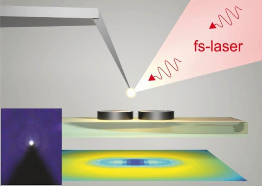
Researchers from ITMO University solved this problem by using the "nanobulb", as they call it, - a miniature light source based on a silicon-and-gold nanoparticle. Its main characteristic is that it emits light in an immensely wide wavelength band: from 400 to 1,000 nm. A single nanobulb can register and analsze the optical response of all kinds of subwavelength nanostructures in the whole visible spectrum at the same time. This increases the efficiency and speed of microscopy by several times.
How it works
To create the nanobulb, scientists from the Department of Nanophotonics and Metamaterials printed a silicon-and-gold nanoparticle. To make it emit light, i.e. emit photons, it is lit with a femtosecond IR laser. Thanks to this energy, electrons first attain higher energy levels, and then "slide" towards the bottom of silicon's conduction band, emitting photons on different wavelengths.
"Silicon, being a nondirect-gap semiconductor, is a poor material for generating emission. In other words, if you light it with a laser, it will absorb maybe a million photons and emit just one. Yet, it is very cheap - you can literally make it from sand. This is why humanity aspires to find as many applications for it as possible: in photovoltaics, microelectronics, and other fields. We have found a most unexpected application, using its main drawback - its indirect band-gap - to create a nano-size source of white light that can emit photons of energy 3.4 to 1.1 eV," - says Sergei Makarov, senior research associate at the Department of Nanophotonics and Metamaterials.
"What is more, at the boundary of these two materials, gold and silicon, interfaces emerge that provide for an even better radiative recombination of electrons. Lots of physical mechanisms that we are yet to research are at work here, so there's a lot of theoretical work that we will have to do to improve our nanobulb, including creating an emittance model," comments Ivan Sinev, PhD student at the ITMO University.
He notes that another positive feature of the nanobulb is that it uses and IR-band laser to generate visible light. This means that extra "noise" in the optical signal can be removed by way of filtering the dissipated IR light, which improves the effectiveness with which the actual signal is registered.
Possible uses
At the suggestion of Anton Samusev, research associate at ITMO University, the nanobulb was placed on a common probe of an atomic-force microscope using a method developed by Ivan Mukhin and Filipp Komissarenko at the Department of Nanophotonics and Metamaterials.
The probe allows bringing the source of visible light immediately near the test subject, which greatly amplifies the interaction of the near fields. The signal from this nanoparticle's emission is registered and separated on a spectrum using a regular spectrometer. T
hus, a nanobulb may be integrated into standard microscopic equipment; in other words, it can be attached to any probe and used to record its signals with regular photodetectors - all while receiving information on a nanoobjects's near-field in the entire visible spectrum band. This means that silicon-gold nanoparticles make microscopy more flexible and cheaper.
"We are also developing an idea of using the nanobulb as a nanolaser. If we place such a particle into a resonator capable of changing the wave's operating length, we can end up with a tunable laser, one that can function at any set wavelength in the visible spectrum. Besides, the nanobulb may also see use in biology for purposes such as 'illuminating' cells and detecting substances that are sensitive to particular wavelengths," - adds Sinev.


