
DNA and lithography used to build optically active structures
US researchers develop method to arrange nanoparticles in two and three dimensions, resulting in optically active superlattices
Northwestern University researchers have developed a new technique for creating entirely new classes of optical materials and devices that could lead to light bending and cloaking devices,
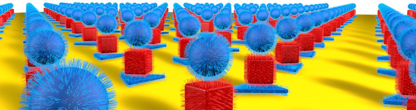
Using DNA as a tool, the interdisciplinary team took gold nanoparticles of different sizes and shapes and arranged them in two and three dimensions to form optically active superlattices.
Structures with specific configurations could be programmed through choice of particle type and both DNA-pattern and sequence to exhibit almost any color across the visible spectrum, the scientists report.
"Architecture is everything when designing new materials, and we now have a new way to precisely control particle architectures over large areas," said Chad A. Mirkin, the George B. Rathmann Professor of Chemistry in the Weinberg College of Arts and Sciences at Northwestern.
"Chemists and physicists will be able to build an almost infinite number of new structures with all sorts of interesting properties. These structures cannot be made by any known technique."
The technique combines an old fabrication method - top-down lithography, the same method used to make computer chips - with a new one - programmable self-assembly driven by DNA. The Northwestern team is the first to combine the two to achieve individual particle control in three dimensions.
The study was published online by the journal Science (Jan. 18). Mirkin and Vinayak P. Dravid and Koray Aydin, both professors in Northwestern's McCormick School of Engineering, are co-corresponding authors.
Scientists will be able to use the powerful and flexible technique to build metamaterials - materials not found in nature - for a range of applications including sensors for medical and environmental uses.
The researchers used a combination of numerical simulations and optical spectroscopy techniques to identify particular nanoparticle superlattices that absorb specific wavelengths of visible light. The DNA-modified nanoparticles - gold in this case - are positioned on a pre-patterned template made of complementary DNA. Stacks of structures can be made by introducing a second and then a third DNA-modified particle with DNA that is complementary to the subsequent layers.
In addition to being unusual architectures, these materials are stimuli-responsive: the DNA strands that hold them together change in length when exposed to new environments, such as solutions of ethanol that vary in concentration. The change in DNA length, the researchers found, resulted in a change of colour from black to red to green, providing extreme tunability of optical properties.
"Tuning the optical properties of metamaterials is a significant challenge, and our study achieves one of the highest tunability ranges achieved to date in optical metamaterials," said Aydin, assistant professor of electrical engineering and computer science at McCormick.
"Our novel metamaterial platform - enabled by precise and extreme control of gold nanoparticle shape, size and spacing - holds significant promise for next-generation optical metamaterials and metasurfaces," Aydin said.
The study describes a new way to organise nanoparticles in two and three dimensions. The researchers used lithography methods to drill tiny holes - only one nanoparticle wide - in a polymer resist, creating "landing pads" for nanoparticle components modified with strands of DNA. The landing pads are essential, Mirkin said, since they keep the structures that are grown vertical.
The nanoscopic landing pads are modified with one sequence of DNA, and the gold nanoparticles are modified with complementary DNA. By alternating nanoparticles with complementary DNA, the researchers built nanoparticle stacks with tremendous positional control and over a large area. The particles can be different sizes and shapes (spheres, cubes and disks, for example).
"This approach can be used to build periodic lattices from optically active particles, such as gold, silver and any other material that can be modified with DNA, with extraordinary nanoscale precision," said Mirkin, director of Northwestern's International Institute for Nanotechnology.
Mirkin also is a professor of medicine at Northwestern University Feinberg School of Medicine and professor of chemical and biological engineering, biomedical engineering and materials science and engineering in the McCormick School.
The success of the reported DNA programmable assembly required expertise with hybrid (soft-hard) materials and exquisite nanopatterning and lithographic capabilities to achieve the requisite spatial resolution, definition and fidelity across large substrate areas. The project team turned to Dravid, a longtime collaborator of Mirkin's who specialises in nanopatterning, advanced microscopy and characterisation of soft, hard and hybrid nanostructures.
Dravid contributed his expertise and assisted in designing the nanopatterning and lithography strategy and the associated characterisation of the new exotic structures. He is the Abraham Harris Professor of Materials Science and Engineering in McCormick and the founding director of the NUANCE center, which houses the advanced patterning, lithography and characterisation used in the DNA-programmed structures.


