A new way to make optoelectronic devices?

Yale researchers integrate oxide 2D electron gases with GaAs to pave the way toward new devices that interact with light
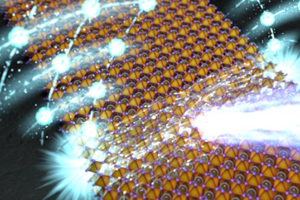
Insulating oxides are compounds that do not conduct electricity, but can nevertheless sometimes form conductive interfaces when they're layered together precisely. The conducting electrons at the interface form a two-dimensional electron gas (2DEG) which boasts exotic quantum properties that make the system potentially useful in electronics and photonics applications.
Researchers at Yale University have now grown a 2DEG system on GaAs, a development that they think is promising for new electronic devices that interact with light, such as new kinds of transistors, superconducting switches and gas sensors.
"I see this as a building block for oxide electronics," said Lior Kornblum, now of the Technion - Israel Institute of Technology, who describes the new research appearing this week in the Journal of Applied Physics, from AIP publishing.
Oxide 2DEGs were discovered in 2004. Researchers were surprised to find that sandwiching together two layers of some insulating oxides can generate conducting electrons that behave like a gas or liquid near the interface between the oxides and can transport information.
Researchers have previously observed 2DEGs with semiconductors, but oxide 2DEGs have much higher electron densities, making them promising candidates for some electronic applications. Oxide 2DEGs have interesting quantum properties, drawing interest in their fundamental properties as well. For example, the systems seem to exhibit a combination of magnetic behaviours and superconductivity.
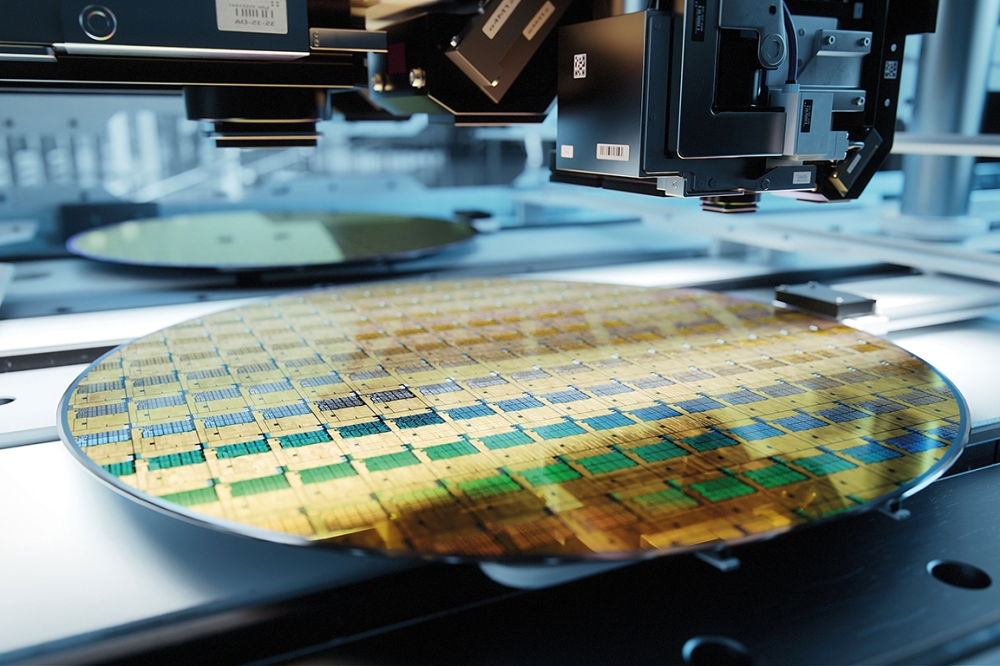
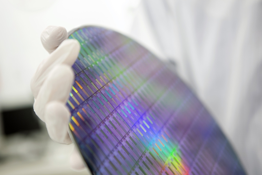
Generally, it's difficult to mass-produce oxide 2DEGs because only small pieces of the necessary oxide crystals are obtainable, Kornblum said. If, however, researchers can grow the oxides on large, commercially available semiconductor wafers, they can then scale up oxide 2DEGs for real-world applications. Growing oxide 2DEGs on semiconductors also allows researchers to better integrate the structures with conventional electronics. According to Kornblum, enabling the oxide electrons to interact with the electrons in the semiconductor could lead to new functionality and more types of devices.
The Yale team previously grew oxide 2DEGs on silicon wafers. In the new work, they successfully grew oxide 2DEGs on another important semiconductor, GaAs, which proved to be more challenging.
Most semiconductors react with oxygen in the air and form a disordered surface layer, which must be removed before growing these oxides on the semiconductor. For silicon, removal is relatively easy - researchers heat the semiconductor in vacuum. This approach, however, doesn't work well with GaAs.
Instead, the research team coated a clean surface of a GaAs wafer with a layer of arsenic. The arsenic protected the semiconductor's surface from the air while they transferred the wafer into an instrument that grows oxides using molecular beam epitaxy. This allows one material to grow on another while maintaining an ordered crystal structure across the interface.
Next, the researchers gently heated the wafer to evaporate the thin arsenic layer, exposing the pristine semiconductor surface beneath. They then grew an oxide called SrTiO3 on the GaAs and, immediately after, another oxide layer of GdTiO3. This process formed a 2DEG between the oxides.
The team believe this work opens a path to integrate oxide 2DEGs with other III-V semiconductors.
"The ability to couple or to integrate these interesting oxide two-dimensional electron gases with GaAs opens the way to devices that could benefit from the electrical and optical properties of the semiconductor," Kornblum said. "This is a gateway material for other members of this family of semiconductors."
'Oxide Heterostrutures for High Density 2D Electron Gases on GaAs' by Lior Kornblum et al; Journal of Applied Physics on January 9, 2018


