
Researchers demo high quality lithium niobate microstructures
Harvard team have designed a micro-ring and micro-racetrack resonators made material previously thought unworkable for high-quality, small scale optical devices
Researchers at the Harvard John A. Paulson School of Engineering and Applied Sciences (SEAS) have developed a technique to fabricate high-performance optical microstructures using lithium niobate, opening the door to ultra-efficient integrated photonic circuits, quantum photonics, microwave-to-optical conversion and more.
The research was published in December 2017 in Optica.
"This research challenges the status quo," said Marko Loncar, the Tiantsai Lin Professor of Electrical Engineering at SEAS and senior author of the paper. "We demonstrated that you can fabricate high-quality lithium niobate devices - with ultralow loss and high optical confinement - using the conventional microfabrication processes."
Lithium niobate is already one of the most widely used optical materials, well-known for its electro-optic properties, meaning it can efficiently convert electronic signals into optical signals. Lithium niobate modulators are the backbone of modern telecommunications, converting electronic data to optical information at the end of fibre optic cables.
But is it notoriously difficult to fabricate high-quality devices on a small scale using lithium niobate, an obstacle that has so far ruled out practical integrated, on-chip applications.
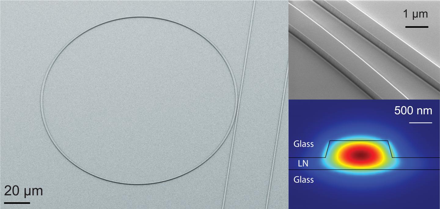
Most conventional optical microstructures are made using processes of chemical or mechanical etching. But lithium niobate is chemically inert, meaning that chemical etching is off the table.
"Using chemical etching on lithium niobate is like using water to remove nail polish, it's just not going to work," said Mian Zhang, co-first author of the paper and postdoctoral fellow at SEAS. "In the past, mechanical etching has also been ruled out because there has been a preconception that lithium niobate is like a piece of rock that can't be sculpted smoothly."
But the Loncar lab -- which is known for their diamond work-- has experience with tough materials. Drawing on that expertise with diamonds, the team used standard plasma etching to physically sculpt microresonators in thin lithium niobate films provided by the company NANOLN.
The researchers demonstrated that the nanowaveguides could propagate light across a metre-long path while losing only about half their optical power. In comparison, light propagating in the previous lithium niobate devices would lose at least 99 percent of light over the same distance.
"The nanowaveguides we demonstrate here have a propagation loss of less than three dB per meter, meaning that now we can do sophisticated manipulation of light over a one-meter path length," said Cheng Wang, co-first author of the paper and postdoctoral fellow at SEAS. "We also show that you can tightly bend these waveguides, so that a meter-long waveguide can actually be packed inside a centimetre-size chip."
"This is a significant breakthrough in integrated photonics and lithium niobate photonics," said Qiang Lin, Associate Professor of Electrical and Computer Engineering and Associate Professor of Optics at the University of Rochester, who was not involved in the research. "This opens the door towards a variety of intriguing functionalities, enabled by the unique optical and electrical properties of lithium niobate that do not exist in in other optical media."
"This research demonstrates that this relatively unexplored material is ready to address critical applications in optical links for data centers," said Joseph Kahn, professor of Electrical Engineering at Stanford University, who was not involved in the research. "Thin-film lithium niobate (TFLN) is uniquely well-suited for any functions requiring modulating light or shifting the frequency of light.? Over the next few years, TFLN will play a key role in enabling tiny, inexpensive, low-power optical modules for data centers to achieve functionality similar to today's telecommunication equipment, which is far larger, costlier, and more power-hungry."
Next, the researchers aim to build on these results and develop lithium niobate platform for a wide range of applications including optical communication, quantum computation and communication and microwave photonics.


