Plessey plans to be first with monolithic microLED displays

Monolithic GaN-on-Silicon displays strategy part of wider plan to become photonic industry's leading technology platform provider
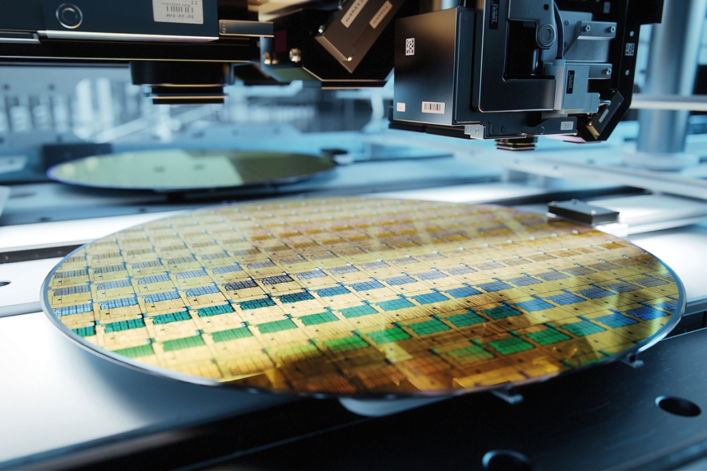
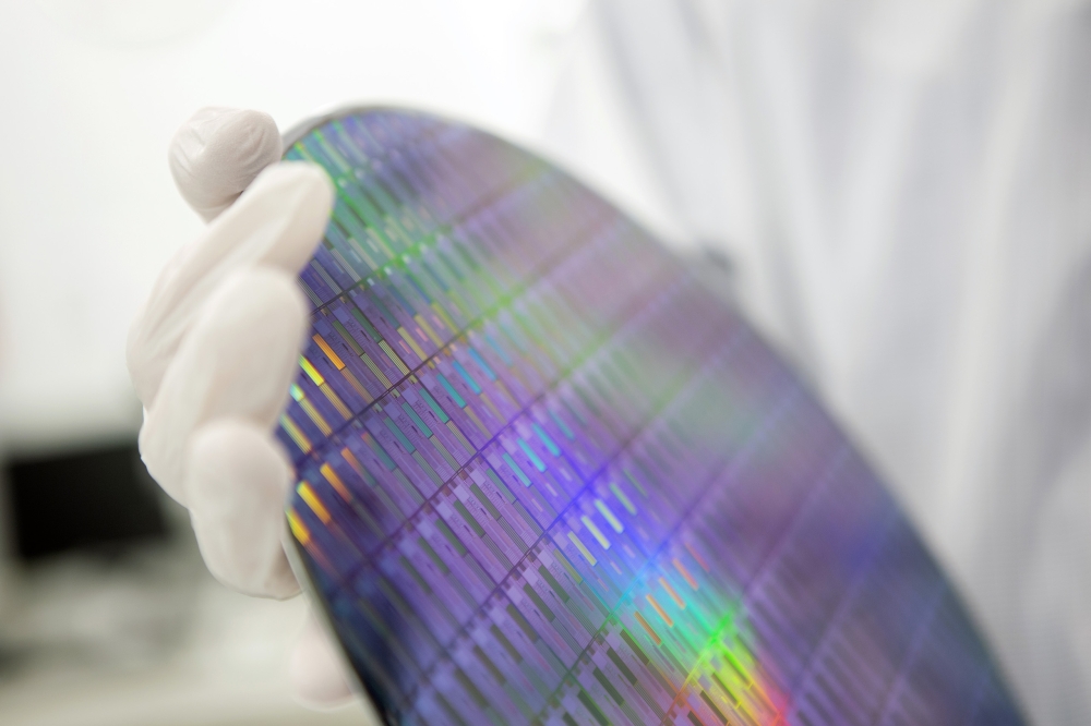
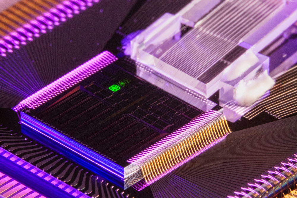
Plessey Semiconductor has committed to being the first to market with a monolithic microLED based display based on GaN-on-Silicon. The company has also started an extensive licensing programme that will see the company license out its GaN-on-silicon expertise to microLED manufacturers in line with its new business strategy of becoming the photonic industry's foremost technology platform provider.
Demand for microLED displays is accelerating with research consultancy Yole Développement forecasting the market could reach up to 330 million units by 2025. GaN-on-Silicon is the only technology platform capable of addressing all of the challenges involved with manufacturing microLED displays in high volumes and cost-effectively, Plessey intends to demonstrate its expertise in the field by being the first to manufacture a monolithic display based on microLEDs fabricated using a GaN-on-silicon approach.
"We made the decision to become a technology platform provider in order to get our technology out to the widest possible manufacturing base to meet this growing demand," explained Michael LeGoff, CEO, Plessey Semiconductor. "By being the first to market with a monolithic microLED display we will be demonstrating our expertise and the ability to access our proven turn-key solution, enabling manufacturers to ramp up the development and production of microLED displays to address emerging applications."
One of the main challenges with manufacturing microLED displays using a non-monolithic approach is the placement of LED chips onto a CMOS backplane, currently achieved using pick and place equipment. This involves the individual placement of every LED on a pitch of less than 50μm, requiring new and expensive equipment that is subject to productivity issues. As the pixel density of displays increases and pitch reduces, pick and place becomes less feasible both commercially and technically.
Moving to a monolithic process removes the need for chip placement and will enable smaller and higher resolution displays for a range of applications, including virtual reality (VR), augmented reality (AR), and head-up displays. As the only monolithic solution commercially available, Plessey's technology doesn't require pick and place equipment and isn't subject to the associated productivity issues.
A fully monolithic approach also supports the integration of the standard CMOS circuitry necessary for driving microLED displays, as well as the close integration of high performance graphic processing units (GPUs), all of which can be carried out using standard CMOS manufacturing methods. By solving all of the major challenges, licensees gain instant access to a technology platform that is ready for volume production.
"GaN on Silicon is the only technology that makes sense in terms of scalability and performance," commented Keith Strickland, CTO, Plessey Semiconductor. "It offers better thermal conductivity than sapphire and higher luminosity than OLED, which is why this technology is widely acknowledged to be the only one that can deliver high resolution, high luminance displays."


