Ayar Labs and GF collaborate on silicon photonics

Companies will develop Ayar's CMOS optical I/O technology as an alternative to copper for data centre interconnects
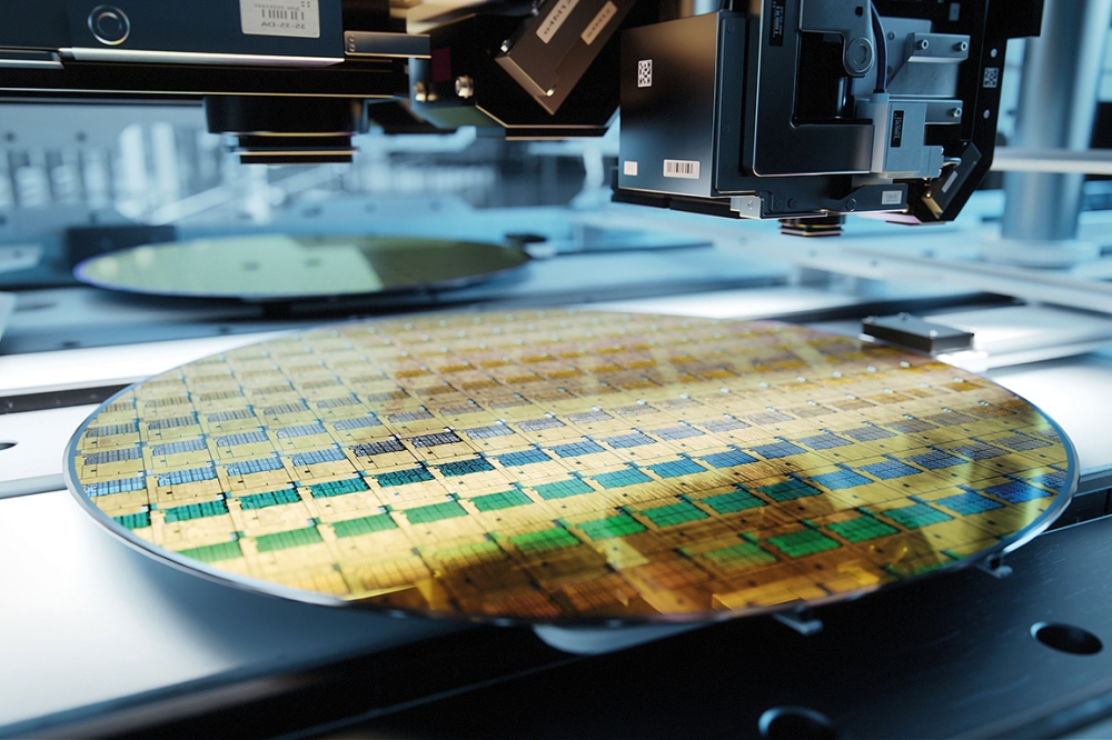
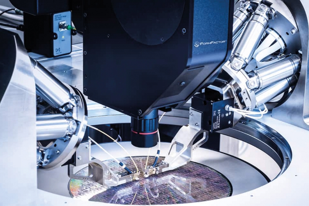
GlobalFoundries (GF) and Ayar Labs, a startup bringing optical I/O to silicon chips, has announced a strategic collaboration to co-develop and commercialise silicon photonic-based devices for data centre interconnect .
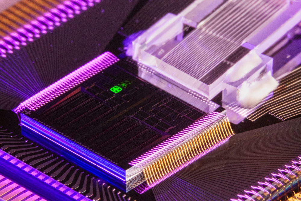
The companies will develop and manufacture Ayar's novel CMOS optical I/O technology, using GF's 45nm CMOS fabrication process, to deliver an alternative to copper I/O that offers up to 10 times higher bandwidth and up to 5 times lower power. T
his solution is integrated in-package with customer ASICs as a multi-chip module, and improves data speed and energy efficiency in cloud servers, data centres and supercomputers. As part of the agreement, GF has also invested an undisclosed amount in Ayar Labs.
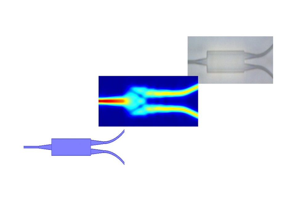
Growth in chip I/O capabilities has not matched exponential increases in computing power, because of physical limitations in electrical data transmission. Optical I/O, which uses optical components on the CMOS die to transmit data at rapid speeds, will help overcome these limitations, particularly in data centre interconnects.
"GF has demonstrated true technology leadership in recognising optical I/O as the inevitable next step as we move into a More than Moore world," said Alex Wright-Gladstein, CEO at Ayar Labs.
"This collaboration between Ayar and GF could improve chip communication bandwidth by more than an order of magnitude and at lower power, and is a validation of Ayar's viability in the current semiconductor ecosystem. This collaboration will unlock a larger market opportunity, expanding both our and GF's customer base. We look forward to working with GF to help solve the interconnect problems of today's chips and create greater value for our customers than if both companies worked independently."
"The Ayar Labs team has been designing cutting-edge silicon photonics components on GF's technology for the past eight years and has achieved exceptional results," said Mike Cadigan, senior vice president of global sales and business development at GF. "Our strategic collaboration builds on our relationship, leveraging GF's silicon photonics IP portfolio and our world-class manufacturing expertise to enable faster and more energy-efficient computing systems for data centers."
The collaboration brings together Ayar Labs' patented IP in optical technology with GF's best-in-class expertise in silicon photonics to co-develop optical solutions that will be fabricated using GF's process technology. The availability of this technology, including certain Design IP cores, will enable internet service providers, system vendors and communication systems to push data capacity to 10 Tera bits per second (Tbps) and beyond, while maintaining the low energy and cost of optical-based interconnects, according to the company.


