
Connecting the worlds of electronics and photonics
University of Twente researcher proposes using 'avalanche mode' silicon LEDs to efficiently bring light on-chip
Electronics and light don't go well together on a standard "˜CMOS' chip. But researcher Satadal Dutta of the University of Twente now succeeds in introducing a light connection into the heart of a semiconductor chip. In this way, two circuits can be isolated and still communicate. Or: the worlds of electronics and photonics are connected.
What is particularly attractive about Dutta's solution is that no special materials or manufacturing processes are needed: the light comes from silicon. The light source, detector and the light channel can be made using the technology that is used to make the electronic circuits. Fully optical circuits are available nowadays, but they use materials like InP and GaAs, which can't easily be combined with the CMOS chip processes used for semiconductor chips you'll find in today's smartphones, for example.
The alternative would be: make a LED light source out of silicon. And that's the problem: silicon only emits a tiny amount of infrared light, while a detector made out of silicon needs visible light. They are talking and listening at different wavelengths. Dutta therefore chooses a remarkable way out: connect the LED in reverse.
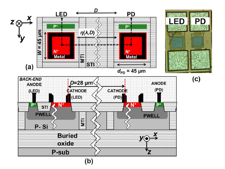
At low voltages, there's no current and light, but at a voltage that is high enough, there will be a small current that amplifies itself like an avalanche. In this "˜avalanche mode', the LED will transmit visible light. Using the same process, the light detector, as well as the light channel in-between can be made. Thanks to the special comb structure that Dutta designed for this, the light source gets more uniform and energy efficient.
An optical link on a chip is a good way to "˜galvanically' isolate two circuits from each other. This is often necessary in cases where one circuit is a low-voltage and low-current one, while the other is a high-power circuit. They should be connected, but not by conducting wires, for reasons of safety.
A classic transformer is an option then, but an optical connection is often used as well. Until now, this is a separate "˜optocoupler', which is large and has limited speed. Dutta's new solution is much more compact as an alternative: it total, it is just a few tens of microns and it offers the protection that's needed at higher bit rates. Compared to optical channels in full-optical circuits, the energy consumption is relatively high, as there is quite some scattering of light.
On the other hand: designing the electronics around the optical link in an efficient way, the amount of light needed for a successful connection, can be kept to a minimum.
All-optical circuits may become the "˜new electronics', predictions say. In the transition from electronic to optic circuits, hybrid circuits, like the one Dutta designed, could play an important role.
Satadal Dutta (1990, Barrackpore, India) did his PhD research in the Semiconductor Components group of Jurriaan Schmitz, together with the Integrated Circuit Design group of Bram Nauta. Dutta's thesis "˜Avalanche-mode silicon LEDs for monolithic optical coupling in CMOS technology' was supported financially by NWO-TTW and NXP Semiconductors.


