
Transfer technique produces wearable GaN gas sensors
Simple production steps could lower cost of producing sensors and other optoelectronic devices, say French researchers
A transfer technique based on thin sacrificial layers of BN could allow high-performance GaN gas sensors to be grown on sapphire substrates and then transferred to metallic or flexible polymer support materials. The technique could facilitate the production of low-cost wearable, mobile and disposable sensing devices for a wide range of environmental applications, according to researchers at Georgia Tech Lorraine in France.
Transferring the GaN sensors to metallic foils and flexible polymers doubles their sensitivity to nitrogen dioxide gas, and boosts response time by a factor of six. The simple production steps, based on MOVPE, could also lower the cost of producing the sensors and other optoelectronic devices.
Sensors produced with the new process can detect ammonia at parts-per-billion levels and differentiate between nitrogen-containing gases. The gas sensor fabrication technique was reported November 9 in the journal Scientific Reports.
"Mechanically, we just peel the devices off the substrate, like peeling the layers of an onion," explained Abdallah Ougazzaden, director of Georgia Tech Lorraine in Metz, France and a professor in Georgia Tech's School of Electrical and Computer Engineering (ECE). "We can put the layer on another support that could be flexible, metallic or plastic. This technique really opens up a lot of opportunity for new functionality, new devices - and commercialising them."
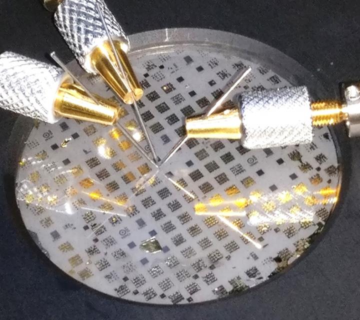
The researchers begin the process by growing monolayers of BN on two-inch sapphire wafers using an MOVPE process at approximately 1,300 degC. The BN surface coating is only a few nanometers thick, and produces crystalline structures that have strong planar surface connections, but weak vertical connections.
Aluminum GaN (AlGaN/GaN) devices are then grown atop the monolayers at a temperature of about 1,100degC, also using an MOVPE process. Because of the BN crystalline properties, the devices are attached to the substrate only by weak Van der Waals forces, which can be overcome mechanically. The devices can be transferred to other substrates without inducing cracks or other defects. The sapphire wafers can be reused for additional device growth.
"This approach for engineering GaN-based sensors is a key step in the pathway towards economically viable, flexible sensors with improved performances that could be integrated into wearable applications," the authors wrote in their paper.
So far, the researchers have transferred the sensors to copper foil, aluminum foil and polymeric materials. In operation, the devices can differentiate between nitrogen oxide, nitrogen dioxide, and ammonia. Because the devices are approximately 100 by 100 microns, sensors for multiple gases can be produced on a single integrated device.
"Not only can we differentiate between these gases, but because the sensor is very small, we can detect them all at the same time with an array of sensors," said Ougazzaden, who expects that the devices could be modified to also detect ozone, carbon dioxide and other gases.
The GaN sensors could have a wide range of applications from industry to vehicle engines - and for wearable sensing devices. The devices are attractive because of their advantageous materials properties, which include high thermal and chemical stability.
"The devices are small and flexible, which will allow us to put them onto many different types of support," said Ougazzaden, who also directs the International Joint Research Lab at Georgia Tech CNRS.
To assess the effects of transferring the devices to a different substrate, the researchers measured device performance on the original sapphire wafer and compared that to performance on the new metallic and polymer substrates. They were surprised to see a doubling of the sensor sensitivity and a six-fold increase in response time, changes beyond what could be expected by a simple thermal change in the devices.
"Not only can we have flexibility in the substrate, but we can also improve the performance of the devices just by moving them to a different support with appropriate properties," he said. "Properties of the substrate alone makes the different in the performance."
In future work, the researchers hope to boost the quality of the devices and demonstrate other sensing applications. "One of the challenges ahead is to improve the quality of the materials so we can extend this to other applications that are very sensitive to the substrates, such as high-performance electronics."
The Georgia Tech researchers have previously used a similar technique to produce light-emitting diodes and ultraviolet detectors that were transferred to different substrates, and they believe the process could also be used to produce high-power electronics. For those applications, transferring the devices from sapphire to substrates with better thermal conductivity could provide a significant advantage in device operation.
Ougazzaden and his research team have been working on boron-based semiconductors since 2005. Their work has attracted visits from several industrial companies interested in exploring the technology, he said.
"I am very excited and lucky to work on such hot topic and top-notch technology at GT-Lorraine," said Taha Ayari, a PhD student in the Georgia Tech School of ECE and the paper's first author.
In addition to Ougazzaden, the research team includes Georgia Tech PhD students Taha Ayari, Matthew Jordan, Xin Li and Saiful Alam; Chris Bishop and Youssef ElGmili, researchers at Institut Lafayette; Suresh Sundaram, a researcher at Georgia Tech Lorraine; Gilles Patriarche, a researcher at the Centre de Nanosciences et de Nanotechnologies (C2N) at CNRS; Paul Voss, an associate professor in the Georgia Tech School of ECE; and Jean Paul Salvestrini, a professor at Georgia Tech Lorraine and adjunct professor in the Georgia Tech School of ECE.
The research was supported by ANR (Agence Nationale de Recherche), the National Agency of Research in France through the "GANEX" Project.
'Gas sensors boosted by two-dimensional h-BN enabled transfer on thin substrate foils: towards wearable and portable applications' by Taha Ayari, et al, Scientific Reports, 2017.


