
Cambridge scientists combine photonics with inkjet printing
Technique enables creation of patterns onto photonic crystals at high speed and over a large area
Researchers at the University of Cambridge and the Hitachi Cambridge Laboratory have successfully combined high-resolution inkjet printing with nanophotonics for the first time. The results are reported in the journal Advanced Materials.
Over the last decade, inkjet printing "“ the same basic technology that many of us have in our homes "“ has advanced to the point where it can be used to print very small devices, using a range of printable materials, including living cells, as "˜ink'. This approach is both simple and low-cost, and it is widely used in electronics and biotechnology.
"Most inkjet printers push the ink through the nozzle by heating or applying pressure, producing ink droplets about the size of the diameter of a human hair," said the paper's co-first author Dr Vincenzo Pecunia, a former PhD student and postdoctoral researcher, and now visiting researcher, at the University's Cavendish Laboratory.
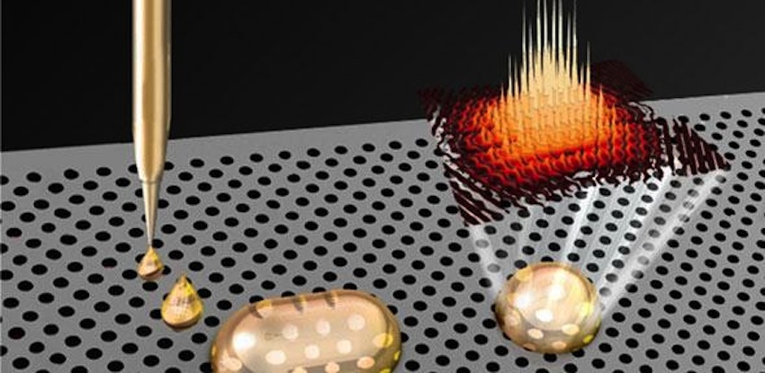
Pecunia's research focuses on printable optoelectronic materials for a range of applications, and his group recently obtained a printer based on electrohydrodynamic jets: a printer capable of ultra-high resolution printing. Instead of relying on pressure or heat, this type of printer applies a voltage to the ink, providing enough force to push it through a much smaller nozzle, producing ultra-small ink droplets "“ ten to a hundred times smaller than those produced by conventional printers.
Thanks to a chance meeting between Pecunia and co-first author Frederic Brossard from the Hitachi Cambridge Laboratory, the researchers found that the new printer could print structures small enough to be used in nanophotonics, which is Brossard's area of research.
"Previous efforts to combine these two areas had bumped into the limitations of conventional inkjet printing technology, which cannot directly deposit anything small enough to be comparable to the wavelength of light," said Pecunia. "But through electrodynamic inkjet printing we've been able to move beyond these limitations."
The researchers were able to deposit ultra-small ink droplets onto photonic crystals. The ink droplets are small enough that they can be "˜drawn' on the crystals on demand as if from a very fine pen, and locally change the properties of the crystals so that light could be trapped. This technique enables the creation of many types of patterns onto the photonic crystals, at high speed and over a large area. Additionally, the patterns can be made of all sorts of printable materials, and the method is scalable, low-cost, and the photonic crystal is reusable since the ink can be simply washed away.
"This fabrication technique opens the door for diverse opportunities in fundamental and applied sciences," said Brossard. "A potential direction is the creation of a high density of highly sensitive sensors to detect minute amounts of biomolecules such as viruses or cancer cells. This could also be a very useful tool to study some fundamental phenomena requiring very strong interaction between light and matter in new materials and create lasers on demand. Finally, this technology could also enable the creation of highly compact optical circuits which would guide the light and which could be modified by inkjet printing using the photonic crystal template."
The research was funded in part by the Engineering and Physical Sciences Research Council (EPSRC) and the Science and Technology Facilities Council (STFC).
"˜Inkjet printed nanocavities on a photonic crystal template' by Frederic S.F. Brossard et al; Advanced Materials (2017). DOI: 10.1002/adma.201704425


