Supporting commercial test and assembly in silicon photonics

Scott Jordan, head of photonics market segment at Physik Instrumente (PI), examines how breakthrough parallel nanoalignment can help PIC makers in speeding up the production of single- and multi-channel photonic devices.
As the world's appetite for data skyrockets, silicon photonics (SiP) promises fresh bounties of bandwidth, scalability and energy efficiency. The transformation of data transmission (and, soon, computational processes) from electronic to photonic is comparable to the development in integrated circuitry five decades ago: It is a fundamental shift that marks a watershed moment in the history of technology. However, there are many challenges to overcome to enable the practical, profitable manufacturing and testing of silicon photonic devices. Escalating demand--combined with the fundamental need for nanoscale-accurate mutual orientation of miniscule photonic elements--necessitates robust, fast automation solutions.
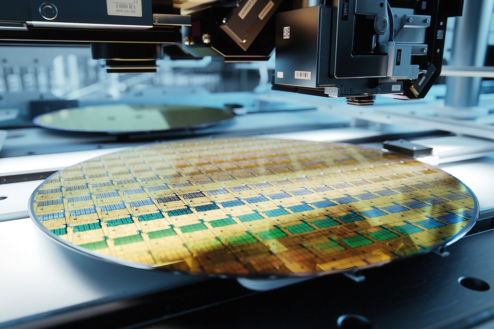
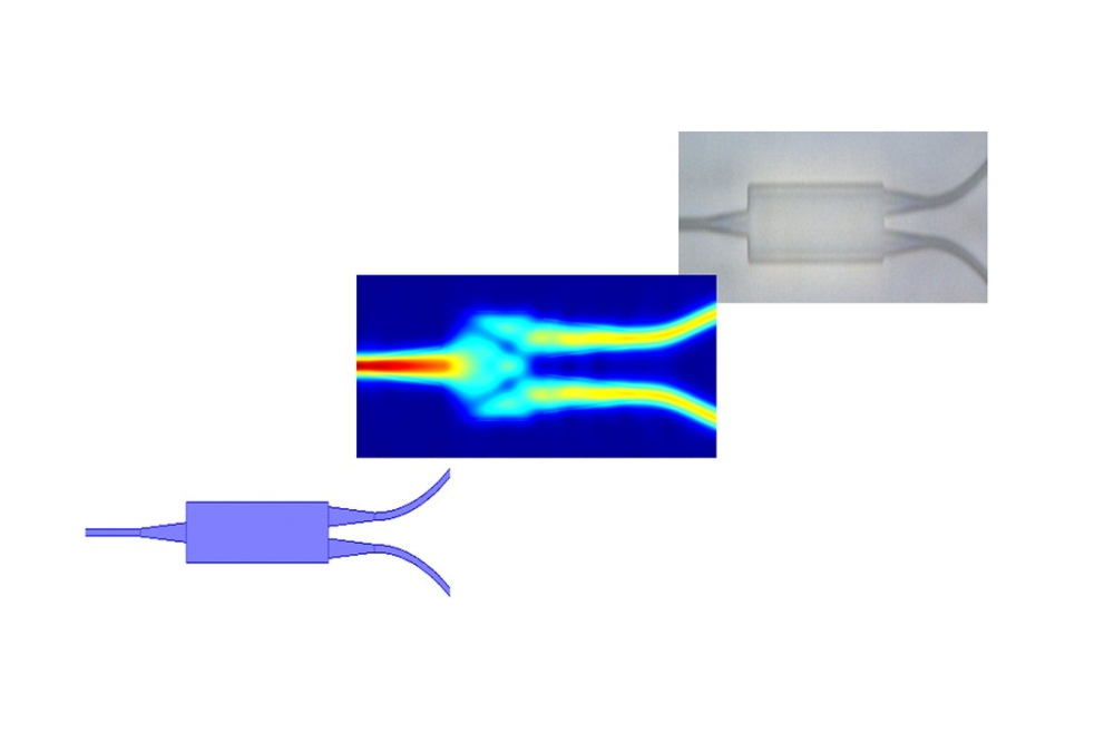
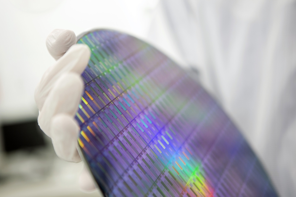
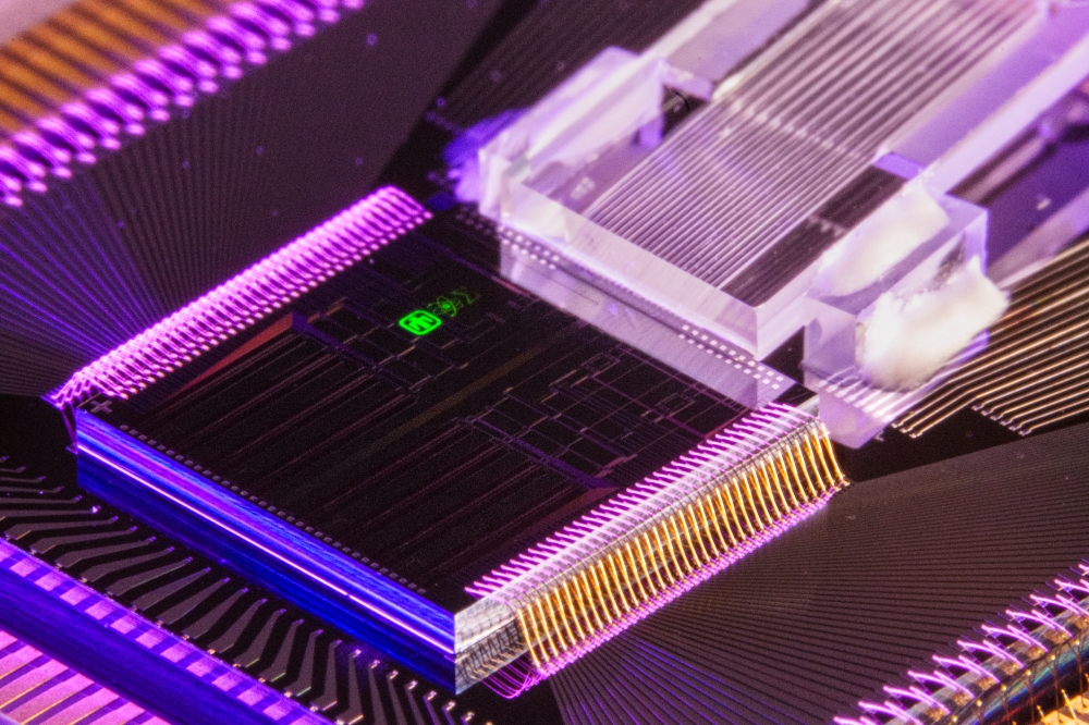
In silicon photonics, optical components are fabricated onto conventional silicon wafers alongside electronic microcircuitry. These components can include sophisticated lasers, elaborate waveguide structures, detectors, modulators, delay and multiplexing/demultiplexing structures, and many other integrated photonic components. The chips are then integrated into packages that can include other chips and active elements plus lenses and other miniaturized optics, plus of course optical fibres and fibre arrays and electrical I/O.
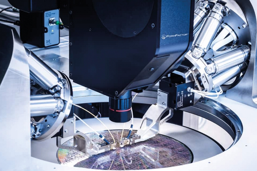
Cascade Microtech's pioneering CM300xi photonics-enabled engineering wafer probe station integrates PI's Fast Multichannel Photonics Alignment systems for high throughput, wafer-safe, nano-precision optical probing of on-wafer Silicon Photonics devices. Photo courtesy Cascade Microtech, a FormFactor company.
Precision alignment of the photonic elements is necessary for this, and for testing the chips to ensure their functionality before the packaging process even begins. Both testing and packaging requires that optical inputs and outputs be coupled to sources and detectors, and all elements must be tested and aligned to each other throughout the optical path to ensure efficient coupling. For today's SiP devices, transverse alignment tolerances of much less than 50 nm are increasingly common. For devices with multi-channel photonic inputs or outputs, additional precision optimization around Theta-Z is needed for efficient coupling of all inputs and outputs of the arrays. It is often the case that Theta-X and Theta-Y orientations also need to be optimized.
Challenges and solutions
These specialized, highly precise and often multi-degree-of-freedom positioning tasks "” repeated multiple times from wafer to final package "” mean the engineer is confronted with vexing geometric effects. For example, adjusting an angle will translate a coupling in X and Y if the centre of rotation is not perfectly positioned (meaning, practically always). In addition, the increasingly commonplace short SiP waveguides exhibit steering effects so that optimization on the input side causes a shift on the output side. That means that the overall best alignment becomes a "moving target". In the past, an iterative approach was therefore necessary to address this and achieve an acceptable, consensus alignment. Above all, this type of process was very time-consuming.
PI has met these challenges and integrated completely new, firmware-based algorithms into its industrial fibre alignment subsystems for fast multi-channel/multi-degree-of-freedom photonics alignment. Designed for integration into production tooling ranging from wafer probing through chip-test to final package, these automated subsystems perform multiple linear and angular digital gradient search optimizations simultaneously.
The resulting parallelism can eliminate the iterative approach formerly required, resulting in process throughput improvements that can exceed two orders of magnitude. Clearly, the impact on production economics and competitiveness is profound. Moreover, the inherent parallelism of this closed-loop, all-digital technology means the overall alignment time in multi-channel/multi-degree-of-freedom applications is only weakly related to the number of individual alignments being performed. For example, in the case of wafer probing operations, it is typical that waveguide I/O coupling is optimized in less than 500msec regardless of the number of inputs or outputs to the SiP chip. Similarly impressive throughput is seen throughout subsequent chip-test and packaging processes.
Designing for a wide range of applications
Because different devices and production applications present different requirements, there are several fast positioning system variants for alignment of single-channel or array devices, with or without angular optimization requirements. All systems are based on very stiff set-ups. If angular optimization is not required, the most popular configuration begins with three stacked precision linear motion stages.
Three-axis alignment system for applications that do not require angular optimization. (Source: PI)
These provide 25mm of travel for coarse positioning and first-light seek. Mounted at the end of this long-travel stage stack, a fast NanoCube positioner provides fast areal scanning motion for mode localization, and fast transverse and Z gradient search capability for dynamic compensation of drift effects, all with nanoscale resolution. Flexure guides and all-ceramic insulated piezo actuators guarantee a long lifetime in round-the-clock industrial deployment. Position sensors on all drives provide microsecond-scale position determinacy, enabling soft limit capability that can safeguard the machinery and costly devices like fully-patterned wafers.
If angular optimization is required, for example when aligning photonic array devices, a parallel-kinematic hexapod is used to provide long-travel, six-degree-of-freedom positioning and first-light seek, plus fast automated angular optimization. These hexapods provide a freely definable coordinate system and pivot point, allowing rotations to be performed about optical sweet-spots such as beam waists and physical channel centres. The NanoCube positioner is again deployed for fine transverse and Z alignment plus dynamic compensation of drift effects and residual geometric errors in parallel with angular optimization processes.
Hexapod-based system with six degrees of freedom for fast and precise alignment of fibres, fibre arrays and optical components. (Source: PI)
The combination of hexapod plus Nanocube provides the foundation for the groundbreaking parallel alignment capabilities of PI's FMPA systems. For example, to align a linear or 2-D fibre array, the NanoCube performs a transverse gradient search with tracking to keep the first channel of the array aligned, while the hexapod performs a parallel theta-Z gradient search on the Nth channel of the array. The hexapod's freely definable center of rotation has already made sure that the optical axis of the first array element can be positioned near to the first channel's optical axis; any small remaining geometrical errors are then compensated by the tracking of the NanoCube. The parallelism of the overall alignment means the entire process is 10-100X faster than previously possible with previous-generation iterative approaches.
Considering production economics
These systems are offered in standard configurations for single- or double-sided alignment tasks, with or without angular optimization. Furthermore, the modular architecture allows additional alignment robotics to be provisioned to meet virtually any applications need. The scope of delivery includes a high-performance digital controller (E-712), the firmware routines with the algorithms for fast positioning and an extensive software package, which covers all application aspects, starting with easy start-up to the convenient control of the systems using graphical user interfaces to fast and manageable integration into external programs.
For systems requiring angular optimization, the hexapod controller (C-887) implements the same scanning and alignment algorithms. These include built-in sinusoidal and spiral areal scans with automatic modeling for accurate peak localization even with fast sparse scans, automatic centroid-determination in top-hat and other challenging couplings, and the unique parallel gradient search processes for one-step optimization across inputs, outputs and degrees of freedom.
Together, these novel subsystems help ensure cost-effective testing and manufacturing of today's silicon photonics devices"” and tomorrow's.


