+44 (0)24 7671 8970
More publications     •     Advertise with us     •     Contact us
 
Loading...
News Article

Ligentec and VLC develop silicon nitride photonic platform

News

Ligentec's process is able to deposit thick film Si3N4 overcoming the challenge of crack formation due to stress in the material

Ligentec, a Swiss provider of manufacturing foundry services in Si3N4 (silicon nitride), and VLC Photonics, a design house offering services for photonic circuit development, have collaborated to offer a generic platform for the prototyping and production of photonic integrated circuits (PICs).

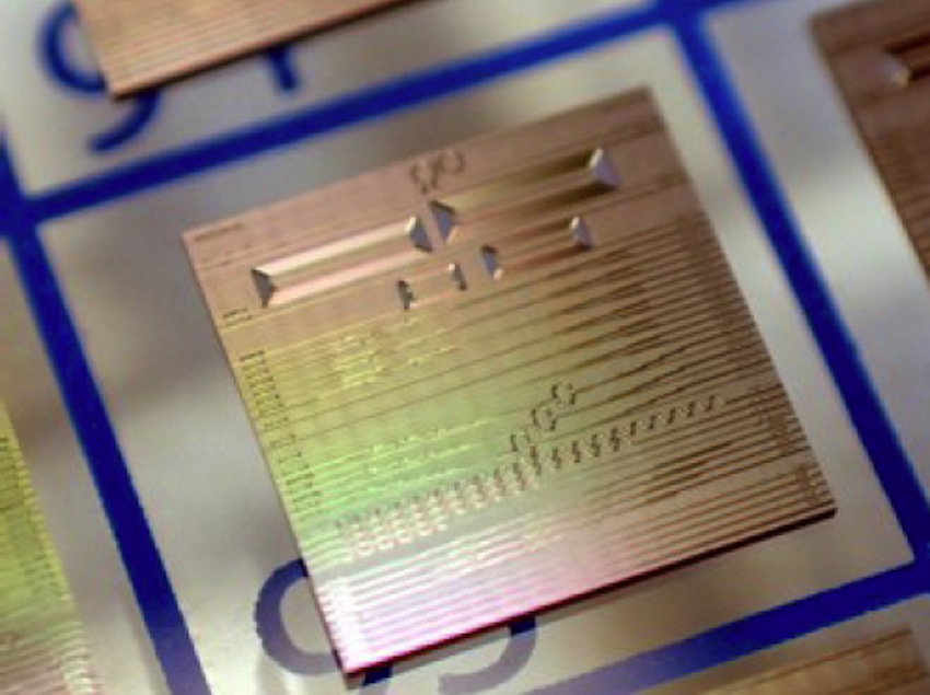
Ligentec has matured a proprietary Si3N4 process that is able to achieve ultra-low propagation losses, with several world record devices being published in the last years. As Michael Zervas, CEO of Ligentec, explains: "Our process is able to deposit thick film Si3N4, from 100 nm to 2500 nm, overcoming the challenge of crack formation due to stress in the material".

The process can also scale up to production volumes using 8 inch wafers and stepper lithography. The open access platform provides a generic fabrication process for designing and manufacturing PICs, to be used in many different applications. Targeting mainly the most common communications wavelengths, the platform is also customisable for lower visible wavelengths, suitable for biophotonic and sensing applications. The main markets addressed are optical telecom and datacom, supercontinuum generation, microwave photonics and quantum optics.

Fabrication is organised through dedicated full-wafer runs or shared multi-project wafer runs, which are periodically scheduled three times a year. Users can subscribe to these runs and prepare their designs using the standardised rules and functional building blocks provided by the foundry and the design house, which have also been implemented under a Process Design Kit (PDK) for two different design software tools, OptoDesigner by PhoeniX Software and IPKISS by Luceda Photonics.

VLC Photonics will also be offering full design or design support for inexperienced users, and also chip characterisation and test services once fabrication has been performed. "We have realized that most of the times, end users also require some level of design or test assistance, to speed their developments and reduce the risk when targeting complex projects", clarifies Inigo Artundo, CEO of VLC Photonics.

EMCORE announces integration of PICs into its products
Scottish photonics consortium wins £4.7m in UKRI funding
Yuanjie Semiconductor to supply lasers to POET
Fraunhofer IPMS announces government funding for quantum photonic chip
POET Technologies partners with Yuanjie Semiconductor Technology
SiLC announces silicon photonics systems for machine vision
Scientists develop novel optical modulators for integrated photonics
Scientists report integrated photodiodes on TFLN
Coherent wins award for innovative photonics product
FBH to present quantum technology developments at EQTC 2023
Skorpios and FormericaOE demonstrate PICs in 800G optical transceivers
EFFECT Photonics verifies fully integrated InP PIC
NASA awards grant for silicon photonics project
OpenLight and Spark Photonics partner on PIC design services
DustPhotonics announces 800G chip for hyperscale data centres and AI
Lightwave Logic Receives Industry Innovation Award
Imec announces SiGe BiCMOS optical receiver
SiFotonics announces silicon photonics 800G LPO solutions
Rockley Photonics progresses noninvasive biomarker monitoring
MantiSpectra secures €4 million for miniaturised spectrometers
Sivers to demo next-gen laser arrays at ECOC 2023
ASMPT AMICRA and Teramount collaborate on silicon photonics packaging
Quantum Computing Inc. selects Arizona site for photonic chip foundry
German government to fund ams OSRAM optoelectronic semiconductor development
Luceda Photonics introduces new PIC design software
Vodafone explores silicon photonics for future mobile networks
Coherent introduces 1200 mW pump laser module
Photonics startups invited to apply to Luminate NY accelerator
New tool could improve lithography for smaller, faster chips
InP-based lasers surpass 2.2 mm
Indie Semiconductor buys Exalos AG
New technique controls direction and wavelength of emitted heat

×
Search the news archive

To close this popup you can press escape or click the close icon.
Logo
×
Logo
×
Register - Step 1

You may choose to subscribe to the PIC Magazine, the PIC Newsletter, or both. You may also request additional information if required, before submitting your application.


Please subscribe me to:


You chose the industry type of "Other"

Please enter the industry that you work in: