Australian researchers develop hybrid glass/silicon photonics chip
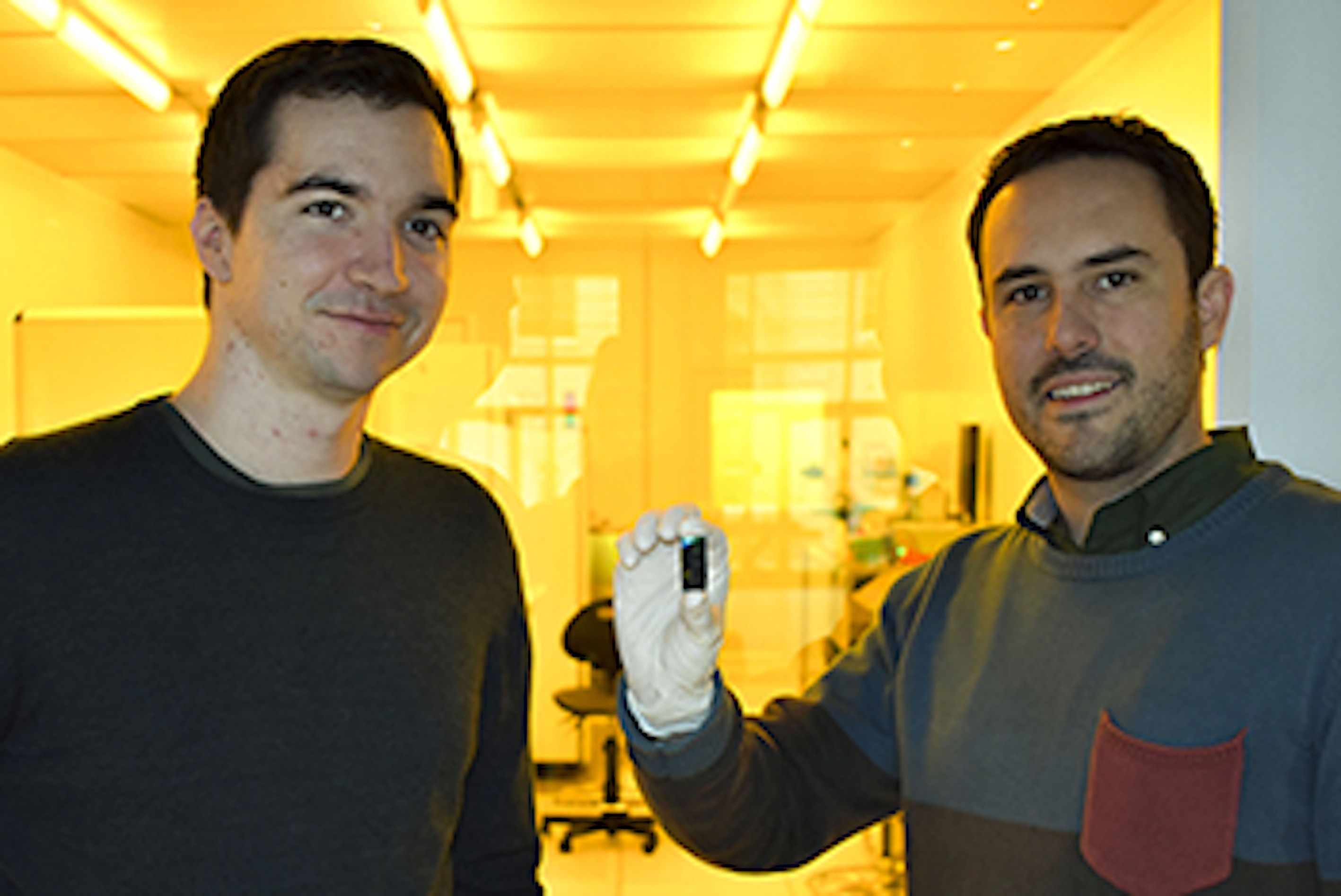
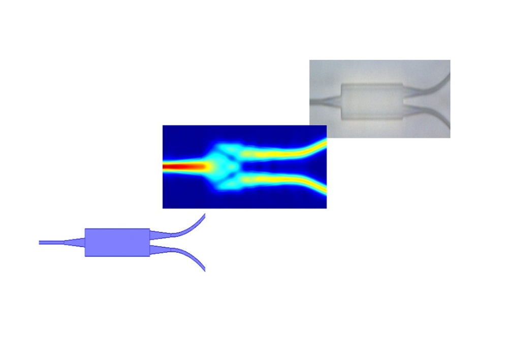
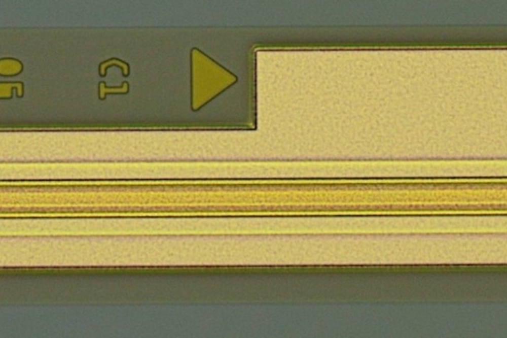
Blair Morrison (L) and Alvaro Casas Bedoya (R) created a compact, optical circuit measuring 0.1 x 4mm, that they say could be mass manufactured and integrated into everyday electronic devices like smartphones
Physicists form the University of Sydney's Australian Institute for Nanoscale Science and Technology (AINST), and its ARC Centre of Excellence for Ultrahigh bandwidth Devices for Optical Systems (CUDOS) have demonstrated optical circuits made of chalcogenide glass and CMOS silicon. The results were published in Optica,Vol. 4, No. 8, August 2017.
Blair Morrison and Alvaro Casas Bedoya created a compact, optical circuit measuring 0.1 x 4mm, that they say could be mass manufactured and integrated into everyday electronic devices like smartphones.
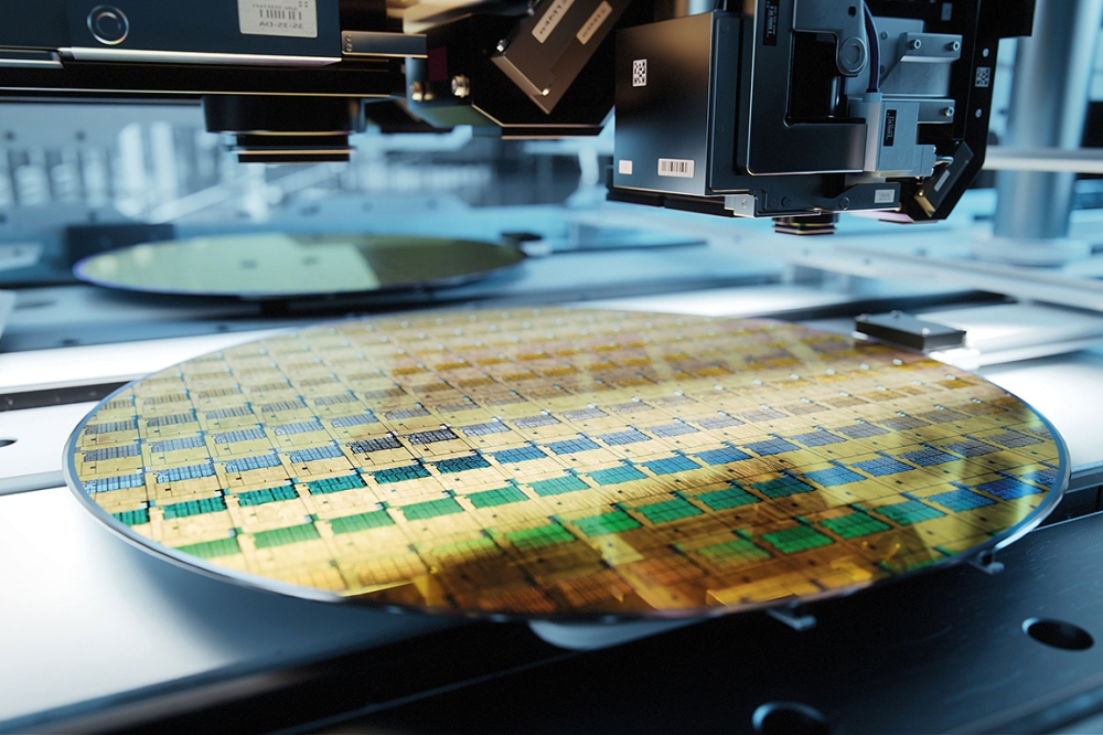
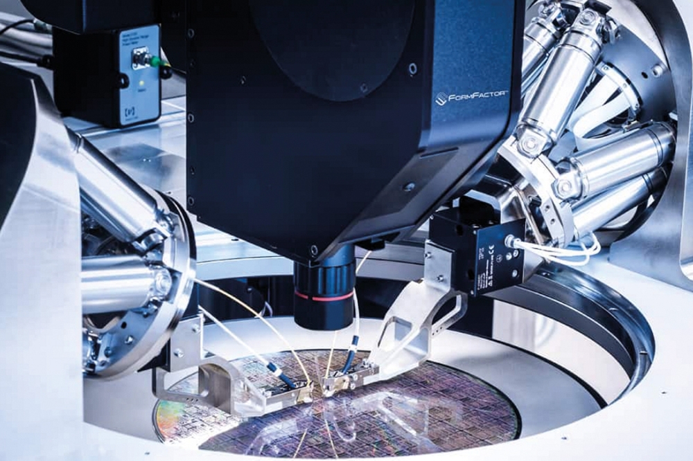
The device was made using silicon wafers from a semiconductor foundry in Belgium, a dedicated facility in ANU's Laser Physics Centre for the glass deposition, and lithography in the RMIT University's School of Engineering. It was characterised and tested in the University of Sydney's AINST.
To showcase the potential of the new approach, the CUDOS researchers further demonstrated a compact novel laser based on light-sound interactions, the first time in an integrated optical circuit.
"In the last few years the group at the University of Sydney has repeatedly demonstrated exciting functionalities, such as broadband microwave devices that can enhance radar, using these novel chalcogenide glasses," Blair Morrison said from the University of Sydney CUDOS node. "Now we have shown it is possible to combine this material with the current industry standard platform for photonic integration, silicon," he said.
"We integrated a novel nonlinear glass into an industrially scalable CMOS compatible platform. We maintained the key advantages of both the silicon and the glass, and made a functional and efficient ultra-compact optical circuit," said Casas Bedoya who is the lead photonics nanofabrication manager for CUDOS.
"This is exciting, because this is a platform which is more compatible with existing semiconductor manufacturing and will allow us to integrate multiple functionalities on a single silicon chip, with active and passive components, such as detectors and modulators, required for advanced applications," said CUDOS Director and ARC Laureate Fellow Benjamin Eggleton from the University of Sydney who supervised the project.


