PLAT4M Matures Three Silicon Photonic Platforms

Accelerates Commercialization of Technology by Linking the Silicon Photonic Ecosystem
Leti announces that the European FP7 project PLAT4M has now been completed offering results which have exceeded expectations.
Si photonics has long been expected to bring substantial breakthroughs in very high speed data communications, telecommunications and supercomputing. In addition, it is one of the most promising industrial-production candidates because of its potential for large-scale and low-cost production capability in existing CMOS foundries.
The European Commission launched the 15-member PLAT4M project in 2012 to build a Si photonics supply chain in Europe that would speed industrialization of the technology by enabling its seamless transition to commercial production.
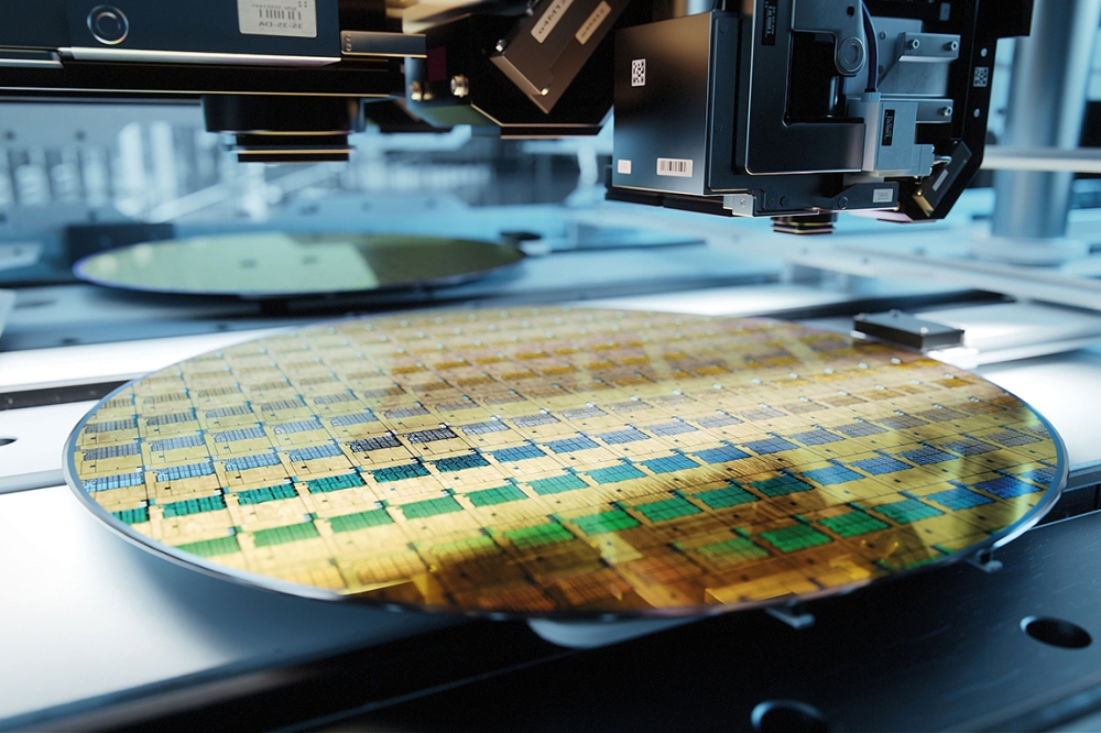
The main objective of PLAT4M was to advance existing silicon photonics research foundries and seamlessly transition to pilot line operation and industrial manufacturing of products based on silicon photonics. The supply chain is based on three different but complementary technology platforms of Leti, STMicroelectronics and imec.
Leti Platform
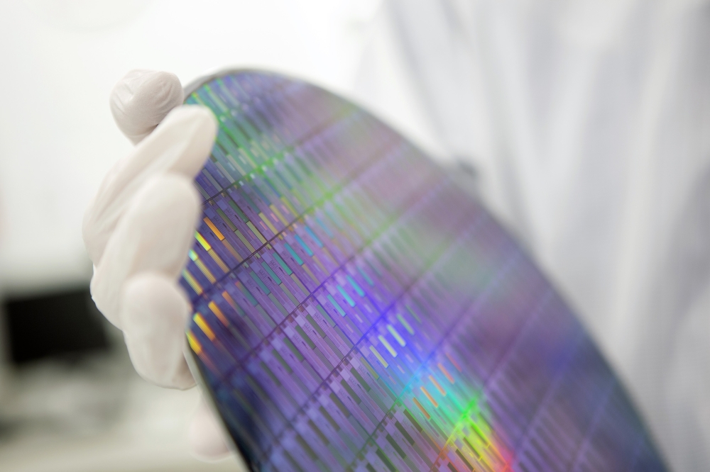
Leti's 8,500m2 cleanroom facility includes a 200mm pilot line that enables fabrication of passives, detectors, modulators and integrated lasers with a focus on high-bandwidth devices. The project team developed a new Si-photonic platform based on a 310nm silicon film on top of an 800nm buried oxide (BOX) on a high-resistivity silicon substrate. Since the targeted applications for the project were O-band transceivers and receivers, most of the developed devices are suitable for 1310nm operations.
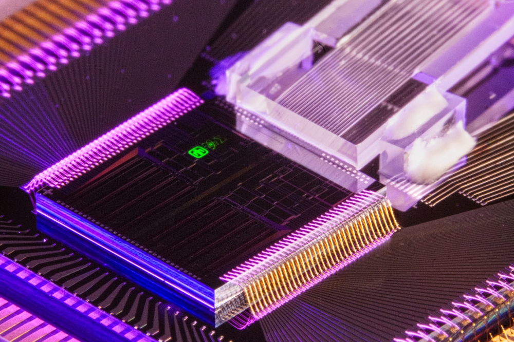
CEA-LETI has developed 3 PDKs which are dedicated to Multi Project Wafers (MPW) runs on this silicon photonics technology which is now offered via the brokers CMP and Europractice. Moreover, III-V Lab has designed and co-fabricated a state-of-the-art integrated hybrid III-V/Si transmitter using a wafer bonding technique on this platform.
STMicroelectronics Platform
STMicroelectronics, the first 300mm wafer silicon photonics device manufacturer, is a key solution provider for 100 Gbps transceiver products since 2016. In parallel to its industrial activity, during the PLAT4M project ST developed another silicon photonics technology aimed at generating and nurturing further application specific industrial nodes. This technology platform creates an advanced photonic nanoscale environment, and combines state-of-the-art CMOS foundry tools with the flexibility necessary to support R&D efforts. Strong collaboration with research partners such as CEA LETI and University Paris Sud have been devoted to advanced studies in power consumption management, optical excess loss reduction and higher data-rate transmissions using complex modulation formats, signal multiplexing and higher Baud-rate devices. With R&D exploration that goes as far as core-to-core optical interposers, ST has also evaluated notions of device and circuit footprints toward Large System Integration (LSI).
In the context of PLAT4M, the participants chose a 4à—25G transceiver as a Wavelength Division Multiplexing (WDM) data-communication demonstrator to validate both LETI and ST R&D platforms. The device functionalities were evaluated for compatibility with the 100GBase-LR4 standard, implying a signal transmission over 4 channels, spaced by 800 GHz around 1310 nm window, one fibre out and one fibre in.
imec Platform
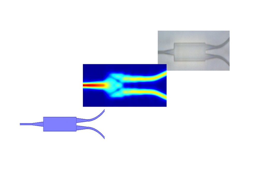
In the course of the PLAT4M project imec has consolidated and further developed its silicon photonics technology platform ISIPP25G using its 200mm pilot line facilities located in Leuven to support industrial prototyping for various applications and markets. The imec platform component portfolio has been expanded to specific devices for sensing and high power free space applications. Furthermore, imec's technology is supporting state-of-the-art modulation and detection at 50Gb/s and beyond with a variety of modulator options (GeSi EAM, Si MZM, Si MRM) now offered under its ISIPP50G technology along with both edge and surface fiber coupling technology and a library of O-Band and C-Band high quality passive components.
The technology is accessible through imec's PDK, which is supported by software tools from several vendors including project partner PhoeniX Software. In collaboration with Mentor, a Siemens business, imec has also explored LVS verifications to reduce design errors and performed litho-friendly design analysis to improve the patterning predictability. Using the imec technology with new processing steps, TNO has demonstrated a multi-channel ring resonator based sensor system. Polytec demonstrated the operation of Multichannel Laser Doppler Vibrometer. THALES has demonstrated an integrated FMCW LiDAR system with 8 switchable output channels, enabling to scanning directions as well as a coherent beam combiner with 16 beams with linear operation up to a maximum input power of 26dBm. The thermal phase-shifter elements achieved a power efficiency of 10mW for a ï°-phase shift.
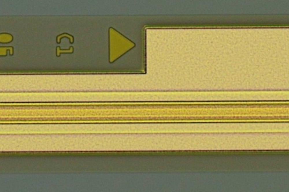
Finally, imec has demonstrated new advances in its technology such as a very low loss silicon waveguide technology (~0.6dB/cm for a 220nmx450nm waveguide) applying leading edge CMOS patterning technology developed in its 300mm pilot line with immersion lithography. It has also demonstrated a further reduction of thermal phase-shifter elements down to 4mW for a ï°-phase shift.
In an Unified Design Environment
The PLAT4M project has led to a qualitative leap of the design flow for silicon photonics, allowing the photonics community to design more complex and more robust circuits. Mentor and PhoeniX Software have worked closely together on an integrated electronics/photonics co-design workflow. This has been accomplished by building on existing tool-sets wherever possible and developing new technologies when required.
The supply chain includes EDA solutions such as Mentor's Pyxi and Calibre, which were extended to "understand" photonics. Interfaces were developed between these tools and Photonic IC design solution OptoDesigner from PhoeniX Software to create integrated design flows using the best practices from both photonics and electronics design. In addition, process design kit elements were developed for Mentor's Calibre DRC, Calibre LVS, and Pyxis tools, incorporating new components, added models and fabrication information.
Producing a Packaging toolkit
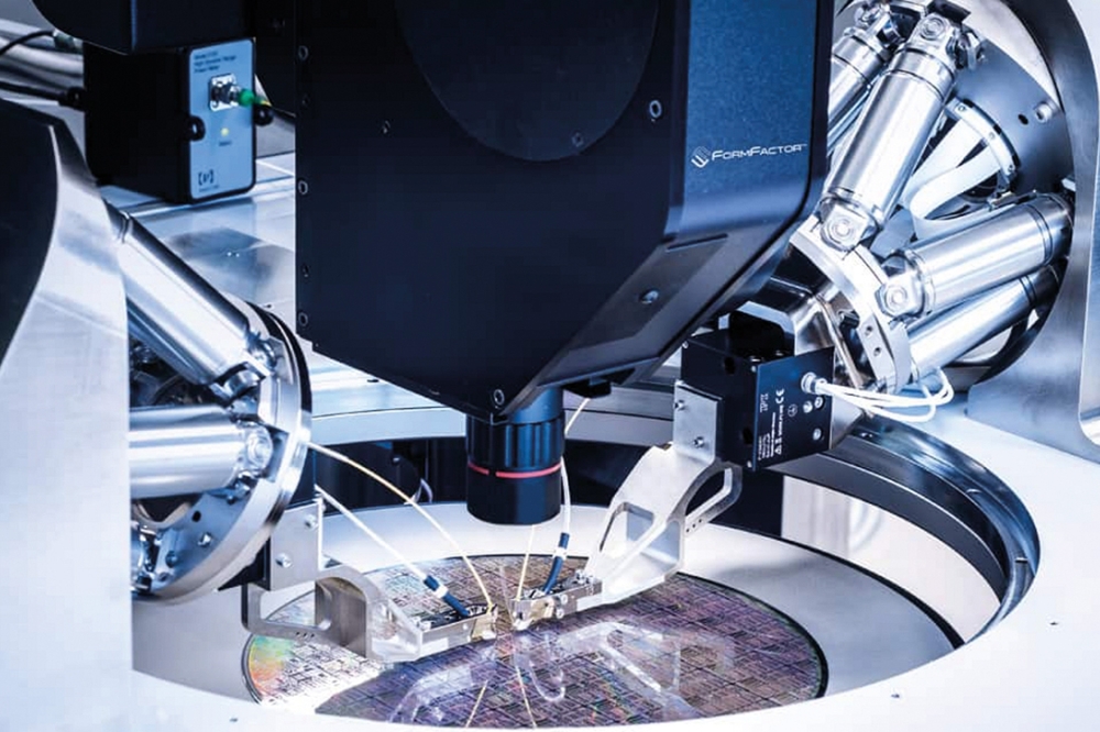
Packaging played a key role in the development of the project demonstrators. The skills and processes developed by Aifotec and Tyndall, advanced the development of the Silicon Photonic packaging toolkit. This toolkit establishes standardised packaging processes for optical fibres, active devices, electronic components and thermo-mechanical systems to ensure that PICs can be more easily packaged in a timely and cost-effective way. A design rule document was made available through EuroPractice by Tyndall and also implemented into PDKs for OptoDesigner.
Perspectives
"The consortium developed advanced technologies and tools by building a coherent design flow, demonstrating manufacturability of elementary devices and process integration, and developing a packaging toolkit," said Jean-Marc Fedeli, coordinator of the PLAT4M project. "The high level of maturity of the technology offered by these platforms makes them readily accessible to a broad circle of users in a fabless model."


