IMECAS develops new Silicon Photonics Platform in China

The Integrated Circuit Advanced Process Center of Institute of Microelectronics of Chinese Academy of Sciences (IMECAS) has recently released a silicon photonics platform based on an 8-inch Complementary Metal Oxide Semiconductor (CMOS) process line, marking a significant increase in R & D capability in the field of silicon photonics in China.
Silicon photonics technology is a new technology developed under the trend of integration of microelectronics and optoelectronics in the post Moore Era. It utilizes mature CMOS technology and platforms, and develops optoelectronic devices and chips based on silicon-based materials.
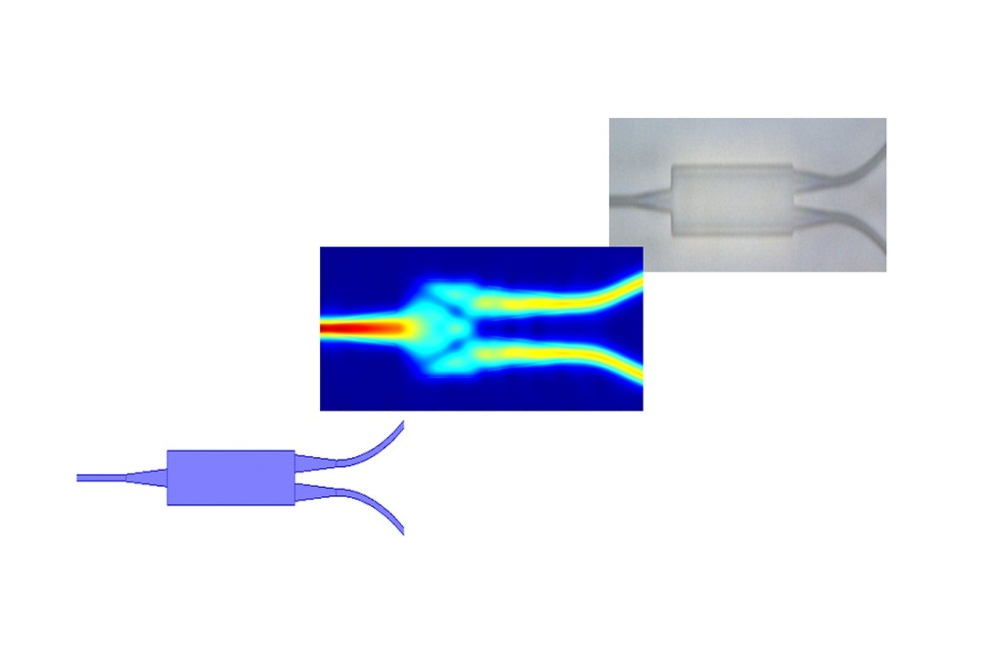
Since 2015, IMECAS has been developing silicon photonics process technologies based on the 8-inch CMOS process line and The Institute has now developed a complete set of silicon photonic process modules. A series of silicon photonic devices including single-mode waveguide, Y branch, optical cross device, coupled grating, tunable attenuator, germanium detector and modulator have been successfully demonstrated.
Silicon photonics is in high demand in the field of optical communication and optical interconnection, but also is considered a potential technology to realize the optical interconnections and optical computing required for the future.
The Process Design Kit (PDK) based on the platform has been released and The Institute is providing the service of Multi Project Wafer (MPW) process for domestic customers.
This silicon photonics platform is one of the first platforms to provide a complete set of process modules for silicon photonic devices in China.
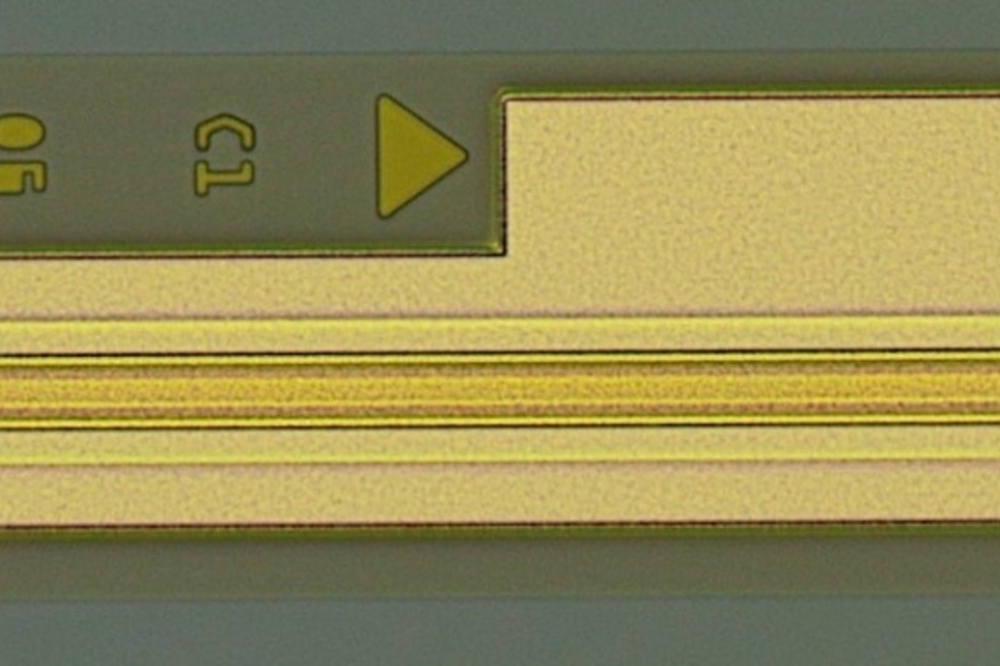
Fig 1. Waveguide (Image by IMECAS)
Figure 2: Y Branch (Image by IMECAS)


