Loading...
News Article

WIN Semiconductors completes second phase of fab expansion
News

Improved compound semiconductor facility features advanced clean rooms and new process lines for optical devices


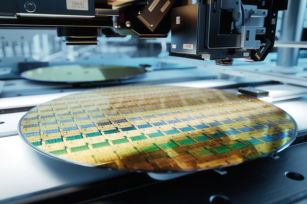
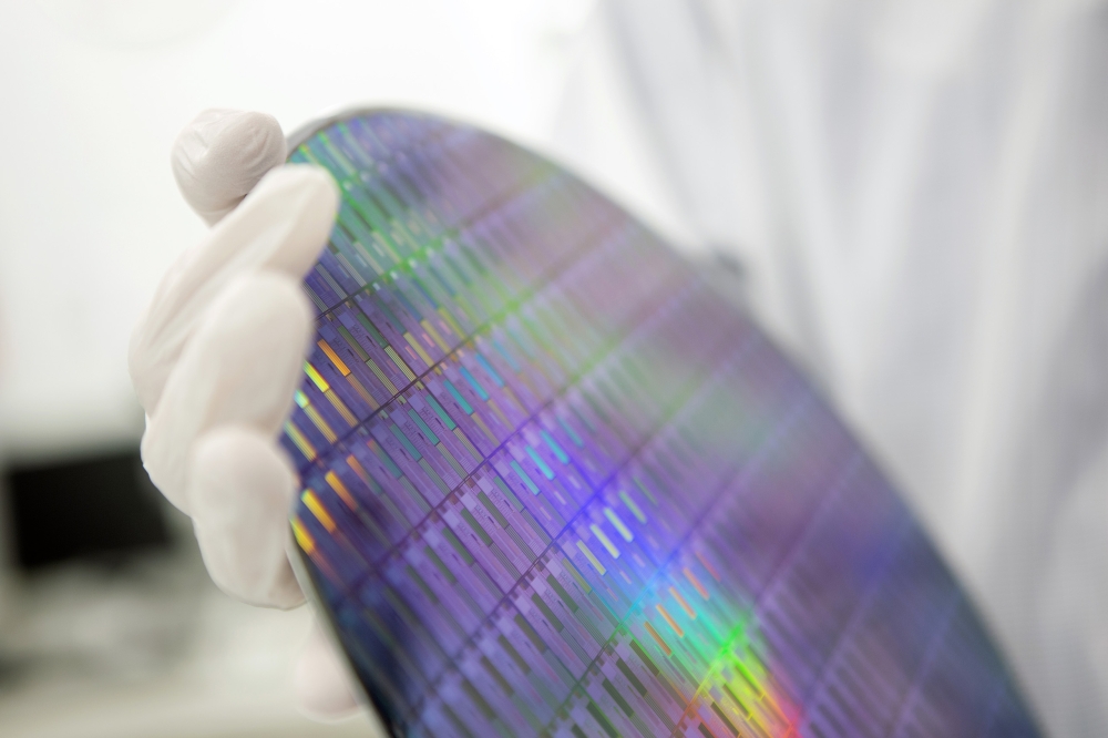
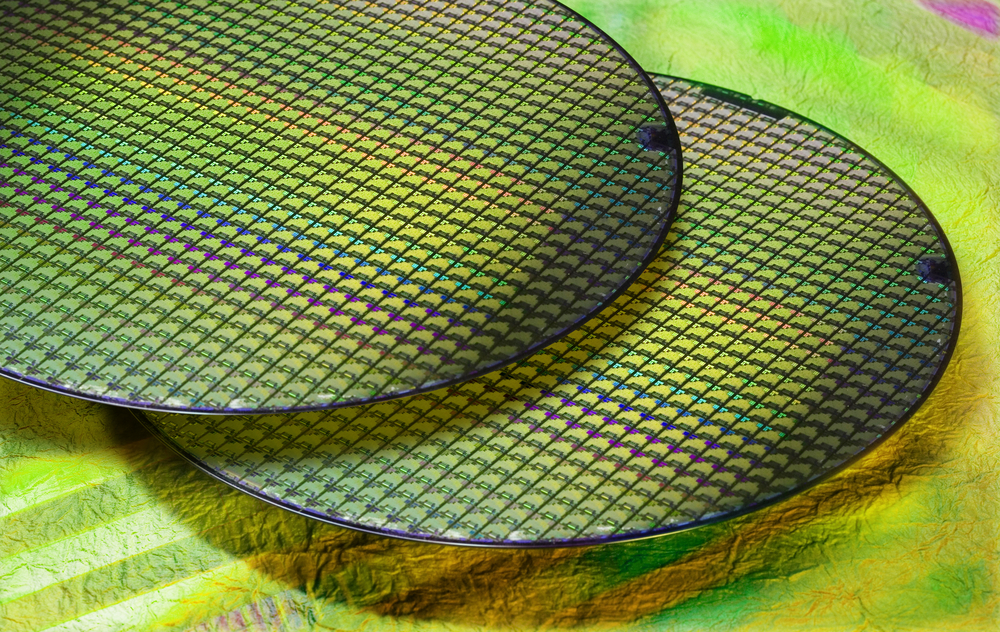
WIN Semiconductors, the Taiwanese compound semiconductor foundry, has completed the second phase of expansion of its newest wafer fab, Fab C. It says this will boost its GaAs wafer manufacturing capacity by over 20 percent.

According to the company, this operation is now fitted with state-of-the-art clean rooms, efficient process lines and advanced equipment for GaAs MMIC production, epitaxial growth of compound semiconductors, as well as fabrication and test of optical devices.

Serving customers in mobile PA, WiFi, wireless infrastructure and optical markets, WINSemiconductors provides a broad portfolio of HBT, pHEMT, integrated BiHEMT technology solutions and optical devices. WIN Semiconductors' manufacturing services can support applications from 50MHz to 150GHz and through light-wave.

"In response toincreasing demand across all market segments, we continue to add manufacturing capacity at our third wafer fab located in Guishan,Toayuan City, Taiwan. Known as Fab C, the facility now supports mass production of a wide range of compound semiconductor technologies. When fully built out, the 706,000ft2 facility will more than double our capacity", said Kyle Chen, senior VP and COO of WIN Semiconductors.

Lightwave Logic receives ECOC Innovation Award for Hybrid PIC/Optical Integration Platform
Coherent wins ECOC award for datacentre innovation
HyperLight announces $37 million funding round
Jabil expands silicon photonics capabilities
Ephos raises $8.5 million for glass-based photonic chips
Designing for manufacture: PAM-4 transmitters using segmented-electrode Mach-Zehnder modulators
OpenLight and Epiphany partner on PIC ecosystem
NewPhotonics and SoftBank team up on advanced photonics
POET and Mitsubishi collaborate on 3.2T optical engines
Integrated photonic platforms: The case for SiC
Integrating high-speed germanium modulators with silicon photonics and fast electronics
Lightium Secures $7 Million Seed Funding
Revolutionising optoelectronics with high-precision bonding
Fraunhofer IMS invites participation in PIC engineering runs
Advances in active alignment engines for efficient photonics device test and assembly
Aeva announces participation at IAA Transportation 2024
Sumitomo Electric announces participation in ECOC 2024
Quside receives NIST certification for quantum entropy source
DustPhotonics launches industry-first merchant 1.6T silicon photonics engine
Arelion and Ciena announce live 1.6T wave data transmission
DGIST leads joint original semiconductor research with the EU
POET Technologies reorganises engineering team
A silicon chip for 6G communications
South Dakota Mines wins $5 million from NSF for Quantum Materials Institute
HieFo indium phosphide fab resumes production
Coherent launches new lasers for silicon photonics transceivers
AlixLabs wins funding from PhotonHub Europe
Sandia National Labs and Arizona State University join forces
Perovskite waveguides for nonlinear photonics
A graphene-based infrared emitter
Atom interferometry performed with silicon photonics
A step towards combining the conventional and quantum internet

×
Search the news archive

To close this popup you can press escape or click the close icon.
Logo
x
Logo
×
Register - Step 1

You may choose to subscribe to the PIC Magazine, the PIC Newsletter, or both. You may also request additional information if required, before submitting your application.


Please subscribe me to:


You chose the industry type of "Other"

Please enter the industry that you work in: