NTT team advances photonics integration

Demonstrates continuous-wave lasing oscillation by sub-wavelength III-V nanowire and high-speed signal modulation by nanowire laser
Photonic integration is still in its infancy. One of the most serious obstacles it faces is the need to use a variety of materials to achieve different functions, many of which aren't compatible with silicon integration technology.
Attempts so far to place a variety of functional nanowires within photonic circuits to reach desired functionalities have shown that, while entirely possible, nanowires tend to be too small to effectively confine light. While bigger nanowires can improve the light confinement and performance, it increases both energy consumption and device footprint - both of which are considered 'fatal' when it comes to integration.
Addressing this problem, a group of NTT Corp. researchers in Japan came up with an approach that involves combining a sub-wavelength InAsP/InP nanowire with a photonic crystal platform, which they report this week in their paper "˜Continuous-wave operation and 10-Gb/s direct modulation on InAsP/InP sub-wavelength nanowire laser on silicone photonic crystal' which was published in the journal APL Photonics.
Photonic crystals - artificial structures whose refractive index is periodically modulated - are at the heart of their work.
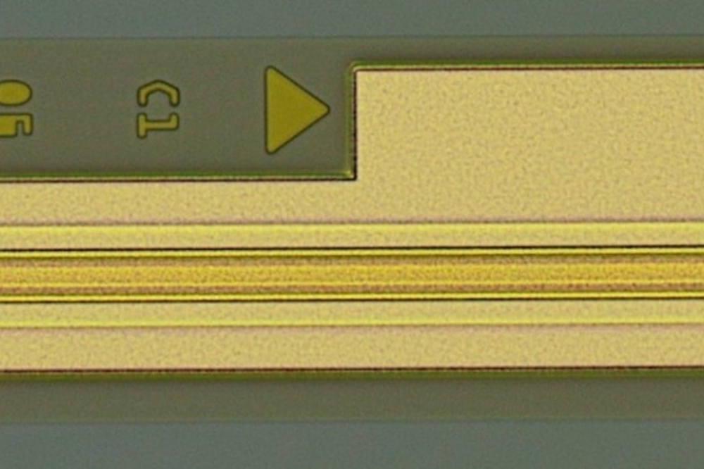
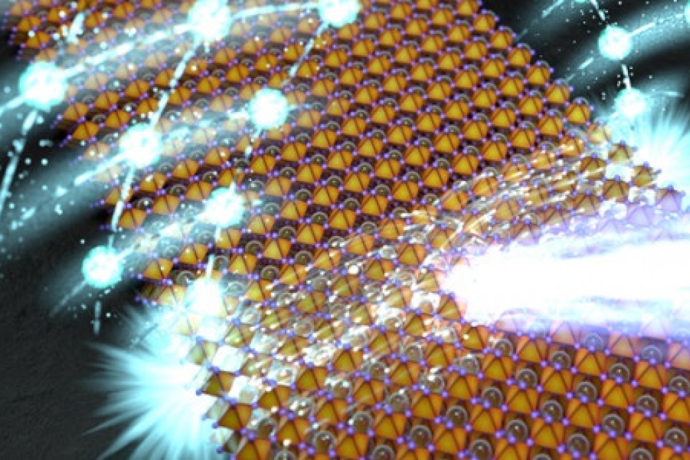
Above: schematic of a nanowire photonic-crystal hybrid laser fabricated by nanoprobe manipulation.
"A small local refractive index modulation of a photonic crystal produces strong light confinement that leads to ultrahigh-quality optical nanoresonators," said Masaya Notomi, a senior distinguished scientist for NTT Basic Research Laboratories. "We make full use of this particular feature in our work."
Back in 2014, this same group demonstrated that it was possible to strongly confine light in a sub-wavelength nanowire with a diameter of 100 nanometers by placing it on a silicon photonic crystal. At that time, "it was a preliminary demonstration of the confinement mechanism, but with our present work we've successfully demonstrated sub-wavelength nanowire device operation on a silicon platform by using this method," Notomi said.
In other words: While a sub-wavelength nanowire can't become a resonator with strong light confinement on its own, when placed on a photonic crystal it causes the refractive index modulation needed to generate the light confinement.
"For our work, we carefully prepare a III-V semiconductor nanowire with sufficiently large optical gain and place it within a slot of a silicon photonic crystal by using the 'nanoprobe manipulation technique,' which results in an optical nanoresonator," said Masato Takiguchi, the paper's lead author and a researcher working within Notomi's group at NTT Basic Research Laboratories. "With a series of careful characterizations, we've demonstrated that this sub-wavelength nanowire can exhibit continuous-wave lasing oscillation and high-speed signal modulation at 10 Gbps."
To use nanowire lasers for photonic integration, three essential requirements must be met. "First, a nanowire should be as small as possible for sufficiently strong light confinement, which ensures an ultrasmall footprint and energy consumption," Takiguchi said. "Second, a nanowire laser must be able to generate high-speed signals. Third, the lasing wavelength should be longer than 1.2 microns to avoid absorption in silicon, so it's important to create sub-wavelength nanowire lasers at optical communication wavelengths - 1.3 to 1.55 microns - capable of high-speed signal modulation."
In fact, previous demonstrations of nanowire-based lasers "have all been at wavelengths shorter than 0.9 microns, which can't be used for silicon photonic integrated circuits - except a pulsed lasing demonstration of relatively thick micron-wire lasers at 1.55 microns," Notomi said. This is presumably because the material gain is smaller at longer wavelengths, which makes it difficult for thin nanowires to achieve lasing.
Beyond this, "zero demonstrations of high-speed modulation by any types of nanowires have materialized," he noted. This is also due to the small gain volume.
"With our present work, we've solved these problems by combining a nanowire and a silicon photonic crystal," Notomi said. "Our result is the first demonstration of continuous-wave lasing oscillation by a sub-wavelength nanowire, as well as the first demonstration of high-speed signal modulation by a nanowire laser."
The group was able to achieve 10-Gbps modulation, which is comparable to conventional, directly modulated high-speed lasers used for optical communications.
"This proves that nanowire lasers show promise for information processing - especially photonic integrated circuits," Notomi said.
The most promising application for the group's present work is nanowire-based photonic integration circuits, for which they'll use various different nanowires to achieve different functionalities - such as lasers, photodetectors, and switches in silicon photonic integrated circuits.
"It's expected that processors equipped with an on-chip photonic network will be needed within about 15 years, and nanowire-based photonic integration will be one possible solution," Notomi said.
In terms of lasers, the group's next target is to integrate nanowire lasers with input/output waveguides.
"Although this type of integration has been a difficult task for nanowire-based devices, we expect it will be much easier in our platform because the photonic crystal platform is intrinsically superior in terms of the waveguide connection," Takiguchi said. "We'll aim for room temperature current-driven lasing as well."
The group also plans to use the same technique to create "photonic devices other than lasers by choosing different nanowires," Takiguchi said. "We want to demonstrate that we're able to integrate a number of photonic devices by having different functionalities on a single chip."


