Building-block approach boosts integrated photonics design
Twan Korthorst, CEO of PhoeniX Software, highlights how "˜Photonic Synthesis' is enabling developers to share foundry resources and ramp up the pace of device development by making the design process much more straightforward.
The integrated electronics sector has been successful in leveraging huge markets using a relatively small set of integration processes (mostly CMOS); and realizing a very broad range of functionality from a small set of building blocks "“ for example, transistors, capacitors, resistors and metal routing (for more details, see "“ "An Introduction to InP-based generic integration technology" Semiconductor Science and Technology, Vol 29, 2014). However, if you look at integrated photonics on the other hand, the story is somewhat different - with fabrication R&D integration efforts optimized for specific applications. This application by application approach can present a hurdle with only a few resulting markets becoming large enough to justify their further development into low-cost production manufacturing ecosystems. Telecoms has historically been the largest PIC market and now datacoms (communications within mega-data centres) seems to be the next.
The question is how to move integrated photonics to the next level of proliferation given the wide variety of integration processes? There are many efforts to integrate some of these processes into so-called generic processes. These efforts will bear fruit over time and will help the industry to consolidate around processes and lower costs. In fact, it may be the integration with CMOS (or some derivative of it) that pushes this photonic sector past the tipping point to large scale adoption. But what do we do in the meantime to help us move the industry forward at a more rapid pace?
Navigating photonic fabrication
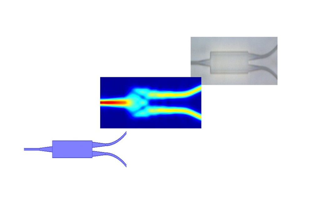
PhoeniX Software of Enschede, The Netherlands, offers a solution dubbed Photonics Synthesis (see Figure 1) that aims to rapidly increase the number of photonic design starts by enabling designers to more easily navigate the multitude of photonic fabrication processes and focus on circuit design instead of the details of semiconductor materials and processes. Provided as a software package (OptoDesigner), the photonics design platform integrates foundry technology information with generic photonic building blocks and proprietary algorithms. The environment provides an easy way for designers to explore the applicability of their design to one fabrication process versus another, enabling designers to eventually target the best fabrication process for their PIC. The key to PhoeniX Software's Photonic Synthesis solution is the ability to hierarchically represent a PIC designer's intent using a library of higher level parameterized building blocks and to then automatically map the design intent into a physical representation (layout) based on a targeted fabrication process.
Figure 1. PhoeniX Software's concept of photonic synthesis
Building blocks for integrated photonics are used to control the basic properties of light: amplitude, phase and polarization. Figure 2(a) shows some of the basic building blocks used for electronic and photonic design while figure 2(b) shows a cross section of the photonic building blocks as implemented in an Indium Phosphide process taken from the COBRA research institute of EU Eindhoven.
PhoeniX Software links together technology information in the form of a foundry process design kit (PDK), analytical and empirical models, simulation engines and photonic building blocks to automatically achieve the mapping of the design intent to the chosen fabrication platform.
Figure 2. (a) Basic building blocks in generic electronic and photonic integration processes. (b) Schematic cross-section of the basic building blocks in a generic photonic integration process.
With basic building blocks that can be used to manipulate amplitude, phase and polarization, and a rich set of higher level generic building blocks such as those shown in figure 3, designers can use PhoeniX Software's Photonic Synthesis to quickly combine these higher level functionalities into fully functional PICs.
Figure 3. Examples of the functionalities that can be realized with (a) passive waveguides devices alone, or in combination with (b) optical amplifiers and (c) phase modulators.
With basic building blocks that can be used to manipulate amplitude, phase and polarization, and a rich set of higher level generic building blocks such as those shown in figure 3, designers can use PhoeniX Software's Photonic Synthesis to quickly combine these higher level functionalities into fully functional PICs.
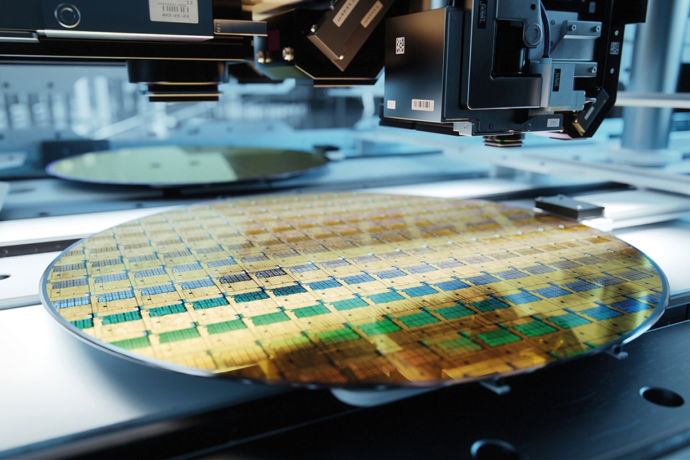
A side effect of standardizing on more generic fabrication processes is that it enables the use of Multi-Project Wafer (MPW) capabilities where a single wafer can be shared by multiple designs since they all use the same process. This lowers the cost of prototyping designs as the cost of the wafer is shared between all of the participants in the MPW run. The approach has been widely used by electronic IC design industry and it is rapidly gaining momentum in Europe and more recently in the United States for photonic designs. PhoeniX Software has been a key enabler for this ecosystem as they provide the engine that links the designers' intent to the foundry processes and MPW runs. PhoeniX Software has worked from the beginning to enable PDK availability from partner companies such as Oclaro, the Fraunhofer Heinrich Hertz Institut, SMART Photonics, VTT, CEA-Leti, imec and now INPHOTEC in Europe. More recently PDK development is also now underway with US-based foundries Sandia National Labs and the AIM Photonic Institute.
As the industry works to move towards more generic fabrication technologies it will be able to justify investments needed for the development of higher performance, better reliability and lower costs. This in turn will enable PICs developed in these processes to be more competitive. The trick is to make it easier for designers to innovate and fill the demand pipeline of the foundries with more designs. The more demand, the more incentive for foundries to invest in generic processes that will enable the market. Photonic Synthesis is key to enabling the creation of more designs and PhoeniX Software is well positioned to be the key supplier of that enabling technology.


