Hybrid PIC integration enables hyperscale data centres
Rob Kalman, director of product management for Kaiam, describes how advances in PIC technology can improve fibre-optic links and open up additional markets
Centralisation of processing and storage in "the Cloud" has resulted in the emergence of "hyperscale" data centres (HDCs). A HDC may contain more than 100,000 high-performance servers densely interconnected to Ethernet switches by fibre-optic links.
The HDCs of internet giants like Google, Microsoft, Facebook, Amazon, and Apple are currently deploying 40 Gbps Ethernet (40 GE) and 100 Gbps Ethernet (100 GE) fibre-optic links. These speeds can only be met economically by using multiple parallel lower-speed channels. For example 100 Gbps is implemented as 4x 25 Gbps today. Another challenge is the large size of HDCs which requires connections of 500 m or more. This combination of increasing speed and length is driving a fibre-optic link migration from one wavelength over multimode (MM) fibre to multiple wavelength division multiplexed (WDM) signals over single-mode (SM) fibre.
These evolving requirements are straining the capabilities of optical transceivers in density, performance, functionality, and cost.
Finding a solution
Photonic integration is the key to meeting the challenging optical interconnect requirements of HDCs. However, practical commercial photonic integrated circuits (PICs) have proven disappointingly elusive since first being proposed by Miller in 1969 [ref: Miller "“ Bell Systems Technical Journal]. Since then, electronic integrated circuit (EIC) densities have increased by more than 109 as predicted by Moore's Law while PIC progress has been modest at best.
There are numerous reasons for this disappointing PIC progress: different optical devices (sources, detectors, wavelength multiplexers, optical switches, etc.) are best fabricated in different materials families; active photonic device materials are much more complex than silicon; photonic device sizes are limited by the optical wavelength to the 1μm range, which is 100x larger than EIC features; and there has been no "killer" application driving massive volumes of high-density PICs.
Hybrid integration
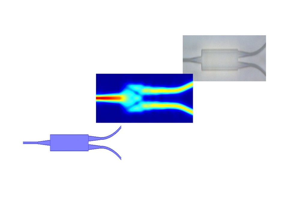
A WDM optical transceiver for an HDC requires a variety of optical devices operating in the 1.3 μm or 1.55 μm wavelength range: laser diodes, photodetectors, and wavelength multiplexers and demultiplexers (note that the transceiver also requires high-speed electronics). The laser diodes and photodetectors are fabricated in the compound semiconductor indium phosphide (InP). By contrast, passive devices like wavelength multiplexers/demultiplexers are best fabricated in inexpensive, low-loss optical materials like silica glass.
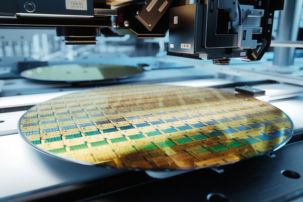
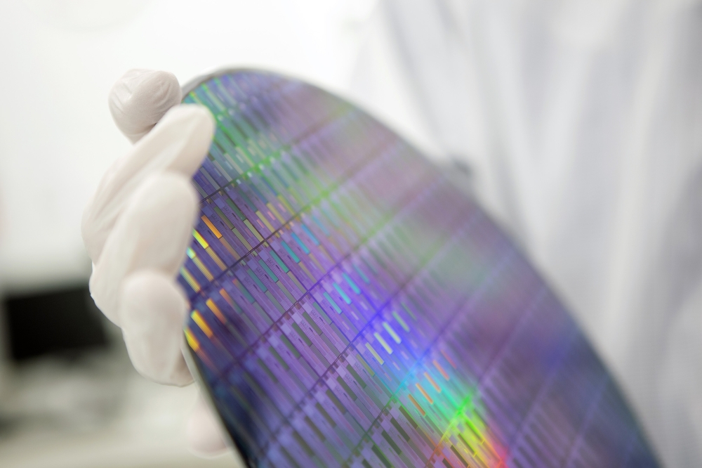
Figure 1. Wafer fabrication: Kaiam has two manufacturing facilities, one in the US and another in the UK. Research and development activities span both sites. Credit: Kaiam Corporation
A "hybrid" WDM transceiver system can combine these different technologies by optically coupling InP PICs containing lasers and photodetectors to silica glass planar lightwave circuits (PLCs) containing wavelength multiplexers and demultiplexers. High efficiency optical coupling from multiple lasers into multiple SM glass waveguides requires "mode matching" the 1µm laser beam diameter to the 9µm glass waveguide diameter while achieving positioning accuracies on the order of 1µm across an array of 4, 8, or more lasers and waveguides. This is a notoriously difficult "holy grail" problem that has impeded the use of hybrid optical integration for decades. Kaiam has finally overcome this hurdle with its - "optical wirebond™" (OWB™) technology.
Making the connection
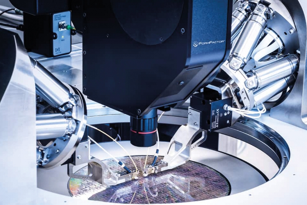
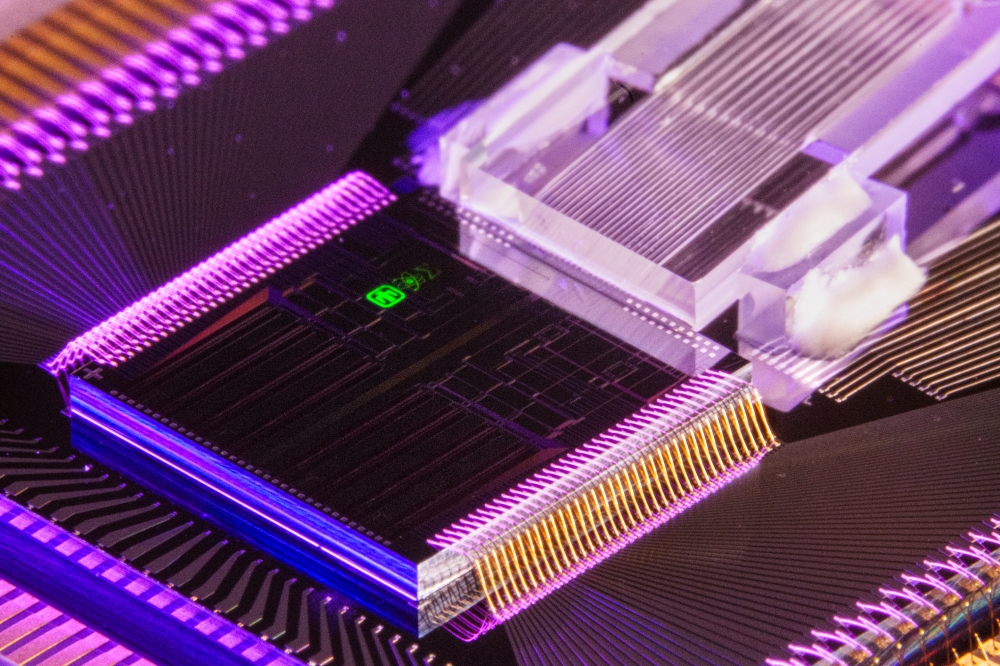
Kaiam's - "optical wirebond™" (OWB™) technology uses an array of microlenses to optically connect PICs and PLCs with high optical coupling efficiency. In HDC transceivers, OWB™ is used to couple a PIC laser diode array to a PLC waveguide array. The microlenses match the laser and waveguide mode sizes to enable low-loss optical coupling. The microlens array is attached to a micro-electromechanical systems (MEMS) platform that can be actively positioned with an accuracy of less than 1µm in a closed-loop process and soldered in place using integrated MEMS heaters. These three parts, namely the InP laser diode array, the MEMS platform and the PLC waveguide are all manufactured at wafer scale and assembled into a hybrid PIC using best-in-class process and materials at each stage. This process is quick and inexpensive, and can be implemented in very compact, robust packaging. An automated OWB™ alignment process, can be used to couple an array of 4, 8, or more lasers to an array of silica PLC waveguides with low optical losses.
Figure 2. OWB™ alignment: The optical wirebond™ process is fully automated and can deliver densely integrated PICs. Credit: Kaiam Corporation
Other markets
There are a wide variety of applications that can exploit PIC for improved functionality, density, performance, and/or cost:
Backbone networks including metro, long-haul, and subsea
High-speed end-user broadband networks such as FTTx and 5G mobile
Displays and gesture capture for augmented and virtual reality user interfaces
Automotive sensing for autonomous cars including LIDAR
Biophotonics
Industrial lasers
It's safe to say we have barely scratched the surface of the potential for hybrid PICs to impact these other applications.
Design and manufacturing
Hybrid photonic integration is a very general approach. It can be applied to a wide variety of integrated photonics technologies: silicon photonics, lithium niobate, polymers, gallium arsenide, etc., in addition to the InP and silica technologies currently being used in Kaiam's products. The OWB™ approach is very flexible and can be applied to interconnect any combination of these technologies.
Hybrid photonic integration leverages decades of investment in the existing semiconductor infrastructure. For instance, Kaiam's silica PICs are fabricated on 8" silicon wafer substrates and use many of the same processing tools used to fabricate CMOS integrated circuits. This fabrication capability is highly automated and scalable to very large volumes.
HDC interconnects will soon migrate to 200 Gbps, 400 Gbps and beyond. The extensibility of hybrid photonic integration and OWB™ will accommodate these increased speed, density, functionality, and cost requirements as a straightforward evolution with no limits for the foreseeable future.


