Building the roadmap of roadmaps: understanding technology needs in 2025-2035
Ton Backx, CEO of PhotonDelta, has a new goal in the coming year. He plans to kick-start international discussions about the optical technologies needed for global society two decades from now. He outlined what's happening and why to Jonathan Marks.
Figure 1. Ton Backx
You can't just guess when things grow exponentially
Photonics is already key to solving the challenges of a modern world. It enhances our quality of life; safeguards our health, safety and security. It is also key to solving the exponential demand for energy coming from the growing number of datacentres. Many technologies are currently exhibiting exponential growth, although it isn't new.
It began 50 years ago, as the age of micro-electronics dawned and powered a wide range of applications. Telecom has proved to be the initiator for exponential growth in integrated photonics applications. We're also seeing similar trends in biosciences and advanced sensors. But without a roadmap, there's a danger that we lose sight of the real-world bottlenecks and challenges ahead.
"We think there's a need for structural discussion on a global basis about a horizon that's 20 years away" says Ton. "If we simply refine current technologies, there is no guarantee that we will meet societal technology demands by 2025, let alone 2035."
So, the sooner we understand more detail about the path ahead, the better.
"Take the tremendous growth in Internet and Telecom traffic. Global bandwidth requirements have exceeded most expectations. Internet bandwidth is expanding with a factor of between 1.5 -1.8 times a year. But whichever figure you believe, if you look at the total traffic that the world needs to handle, within 10 years it means is 600-fold increase in the bandwidth needed to cope with it all. Or things come to a grinding halt."
Technology Breakthroughs in Eindhoven
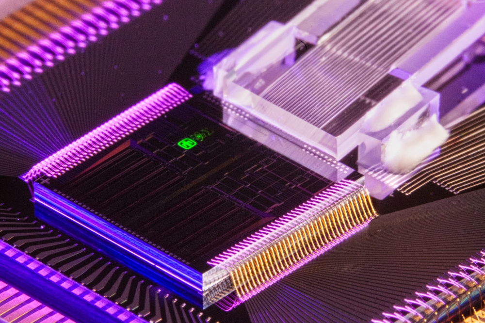
"But there is hope coming from ongoing research. In our labs at the Institute for Photonic Integration in Eindhoven, for instance, we've built a working demonstrator which can communicate at a speed of 255 Terabits per second. By comparison, in today's commercial long-haul optical fibre connections, the maximum speeds applied are around 0.16 Terabit per second.
Since we estimate that bandwidth needs within a decade will be around 600 times greater than today, then we know that we have a good chance to develop this technology in time to meet market demand. And we can also make more accurate projections on the energy required to power the datacentres when they are called upon to handle that kind of traffic.
We often forget that it can take anything between 10-15 years to go from an idea in a lab into a technology that a manufacturer can build in medium - or large quantities. And we know we cannot do this in isolation.
Importance of the long-term view
As a global society, we need to look ahead 15-20 years. We need to carefully examine the projections to work out which technologies we will require. Is there a gap between what is expected by industry and what research organisations believe is feasible to deliver within that timeframe?
Perhaps the biggest proponent of the long-term view is Amazon CEO Jeff Bezos. "If everything you do needs to work on a three-year time horizon, then you're competing against a lot of people," Bezos told Wired in 2011. "But if you're willing to invest on a seven-year time horizon, you're now competing against a fraction of those people, because very few companies are willing to do that."
Ton Backx continues. "It's true, several optical science research teams on both sides of the Atlantic have been developing roadmaps looking 5-10 years out. They are doing important work. But, in our opinion, they don't go far enough or have a broad enough scope to ensure you detect major technical challenges and roadblocks early enough. We are currently setting up a procedure to change that."
Two types of workshops
Figure 2. Active workshop session
"I am currently drawing up a plan of how these roadmaps would be built. We're aiming to make them into living documents, revised on an annual basis. In that way, they can keep track of the real-world trends and adjust accordingly. We also need to ensure that the procedures to do this will stand for several decades."
"We're planning to do this with two types of active workshops to be hosted in The Netherlands next year.
"In March 2017, we will have a preparatory meeting for the first main workshops. We're inviting 10-12 of the world top experts who cover research and development in key technologies. These specialists understand where we are in applied technologies and hurdles that still need to be solved before manufacturers in the private sector can take over. This preparatory team is tasked with the preparation of the first global long-term roadmap development conference."
"We expect the main workshop to be held in the Netherlands in June 2017 involving around 150. These people will come both from research as well as industry. The first workshop will be invitation-only to ensure we can refine the topics that require attention in the roadmap. But once established, the subsequent workshops in 2018 and beyond will be open to anyone who can actively contribute and is willing to participate."
"We need to better understand what the market expects and the specific technology needs. What can be done to lower the cost of the technology to the tipping point where there is widespread adoption? How complex are the challenges to be solved two decades from now?"
Photonics Chips are a good example
"In other sectors like healthcare we're seeing ambitious roadmap programs being launched. The US National Cancer Moonshot, for instance, has set a goal of doubling the rate of progress "“ to make a decades' worth of advances in five years."
"We will probably cast the horizon even longer - 15-20 years ahead. And certain big challenges require several steps in between the 5-year forecast and the 20-year projection."
"Another example is the photonics integrated chip. Currently, chip-design companies can put up to 2000 components integrated onto a single chip. By 2025, and applying the exponential growth factor, we would expect 100,000 devices on a chip of similar size."
"But as you shrink the size and increase the integration density of components, there comes a point where you start to see interactions between them which may have consequences for the performance. Components may need to be isolated, and at the moment we don't have a way to do this. There are thoughts on materials, but nothing firm. We need several years to solve these issues to reach our goal."
Understanding complex paths
"Roadmaps also help to judge the complexity of the problem. It may be that research and development projects can be coordinated to run in parallel, or an application put on hold until a supporting technology has reached a given milestone. In the end, it gives a clearer picture of the priorities and where investment can best be channelled for maximum effect.
We're also extending the invitation to other sectors which include nanotechnology groups working on advanced photonic sensors in life sciences, agriculture and forestry, as well as autonomous vehicles and big data science. I am currently preparing an initial discussion document and welcome thoughts from the community. The structure is going to be important because we hope it sets a framework for discussions that can continue for a long time. I see it as complementary to the important debates taking place in Brussels at PIC International.
I've also been pleased by responses from industry specialists who see the need for roadmaps. From their perspective, the hardest challenge is to identify which intellectual property is worth investing in, what IP are others expected to develop and how do they match."
Outreach to other hotspots has begun
Figure 3: Bert Pauli
PhotonDelta has received full backing from regional government in this endeavour. Bert Pauli is vice governor Economics and International affairs for the province of Noord-Brabant. He has a heritage of working in industry and always understood the need for international outreach.
"The South-Eastern part of the Netherlands has always been a world-class high-tech hub, conducting pioneering research into optical devices and integrated circuits. It's where Philips invented the Compact Disc and the DVD. Related enterprises have also sprung up "“ the region is home to ASML, the world's largest supplier of machines to manufacture chips as well as Holland's leading business park, High Tech Campus Eindhoven."
"The secret to ASML's success lies in their ability to work with 2400 small and medium enterprises. All these companies share a common goal - to produce the best quality goods and services in new, agile and clever ways. In this region, we have pioneered methods to ensure open, trusted and transparent collaboration. And now that's paying off. We've succeeded in accelerating innovation in sectors such as aerospace, pharmaceuticals, and logistics - all sectors which have traditionally been very closed. On December 1st 2016 we opened the Jheronimus Academy of Data Science. Developments in Big Data analysis are going to need quantum computing speeds and security. And photonics has many relevant technologies to achieve this."
Government as a public entrepreneur
The role of Brabant regional government is increasingly a form of "managed serendipity".
"We see a growing need to be far more forward thinking, anticipating what's coming - not what's already been discovered, "continues Pauli.
"We maintain a "helicopter view" because individual sectors often get locked into their own circles. We see connections emerging between photonics, robotics, healthcare and data science. By keeping an active dialogue going with large and small companies as well as the many research institutes we have close-by, we're able to trigger opportunities that they cannot see themselves."
"Earlier this year, we supported the launch of PhotonDelta, which we see as an important international initiative connecting the research communities with high-tech enterprise and investors. A vibrant ecosystem has quickly established itself because all the elements needed for innovation are very close by. In helping to form PhotonDelta, we quickly recognised the need for alliances beyond our region. In the Dutch province of Twente for example, the MESA+ Nanolab, LioniX International, PhoeniX Software and the University of Twente have each developed important photonics technologies which complement the work being done in North Brabant."
"We're also grateful for the outreach assistance we're getting from the innovation attachés at the Netherlands embassies abroad. They are important in our efforts to explain the need for these long-term technology roadmaps."
Realising our preferred future
"There no doubt in our minds. We've entered a new era for photonics. Public investment is still needed to bridge the gap between working prototypes leaving the research lab and the point at which the chips are ready to be manufactured in quantity. It's at that point where the private enterprise takes over."
"We're an active participant in the Vanguard Initiative. It has grown into an excellent example of 30 of Europe's smartest regions collaborating on the grand challenges facing our planet. And what we've learned by working closely with companies and institutions in Baden-Wuerttemberg, Germany, Flanders, Belgium, and Emilia Romagna, Italy, is now being applied elsewhere."
"With Photonics, we're currently reaching out to the leading technology hubs in the world. We have already received interest from organisations like the American Institute for Manufacturing Integrated Photonics and the International Consortium for Advanced Manufacturing Research (ICAMR) based in Central Florida. And in the last few weeks, companies in several parts of Europe as well as China, Singapore, Taiwan and Israel have shown interest in actively supporting us."
"Photonics has already been chosen by the European Commission as one of the 6 key enabling technologies - now we're ensuring that the workshops we set up next summer will be open to anyone who can actively contribute and participate. Knowing what's going on and what needs to be done for the future is in everyone's interests."


