Q&A: Transforming ideas into innovations
The network of Fraunhofer Institutes, which has links all over the world, explores a variety of applied research themes across a range of disciplines. James Tyrrell interviews Martin Schell, director of the Fraunhofer Heinrich-Hertz-Institute (HHI) Berlin, to discover more about its work in the area of photonic integrated circuits, and find out how his team works with industry to develop promising concepts to the level of manufacturing maturity.
To help set the scene, can you summarise the role of the Fraunhofer HHI and where it sits between academia and industry?
The Fraunhofer Society's mission is to partner with companies to transform original ideas into innovations that benefit society. As one of 66 Fraunhofer institutes, HHI researches various aspects of information transmission, ranging from video compression over wireless networks to photonic components and networks. We derive ~50% of our budget from direct industry contracts. The majority of these contracts target a time-to-market below three years. Here, we either develop our own designs or co-design new products with industry partners. We also offer measurement and test services and prototype packaging.
Fraunhofer's role is somewhere between academia and industry: academia often focuses on work with large potential for scientific publications. At HHI, however, a large share of our work is devoted to bringing existing concepts to manufacturing maturity. Our researchers have much experience in that due to the wide range of different products in our history. Our industry partners also have the option for pre-series production on our ISO-certified Indium phosphide or polymer lines, so that transfer to high volume lines can be pushed out to later times - when both the market success of the new product is proven and the production has reached a certain stability. Compared with industry, we focus much more on maintaining scientific excellence over several decades rather than high year-to-year revenue growth.
When did you first notice the impact of photonic integrated circuits and how have you seen the technology progress?
From 2000 to 2002, I was product line manager for FTTH at Infineon Fiber Optics. This included BIDIs, a product that separates incoming 1550 nm light from outgoing 1300 nm light. It was first demonstrated by Infineon in the mid-1990s and contained two TO cans, a thin-film filter, a ball lens and various mechanics, which were combined in about 30 manual assembly steps. Market volume was in the 10s of millions. Over the years, a couple of companies developed photonic integrated circuits, and all failed. This made me quite skeptical when I started at HHI in 2005. Nonetheless, in 2007 we started research on a monolithically integrated 90° hybrid for coherent reception, which later turned out to be a huge commercial success. Here, discrete optics seems to be fully eliminated from the market. So, if you want to have impact with your idea for a PIC, be sure to analyse the market demand, your strengths and weaknesses, and the further evolution of the incumbent technology very carefully.
Overall, I am pretty sure that photonic integration -- sooner or later -- will dominate Telecom and Datacom. I see the largest potential for PICs to not only replace discrete optics, but also to grow the market, in 3 cm to 30 cm data transmission (where PICs could replace today's copper solutions) and in sensor applications. The technology advancement in PIC technology in the last 5 to 10 years has been huge. The fact that there are multiple activities, which have helped to significantly lower the entry threshold for the non PIC savvy developers, is of importance too. Two prominent examples are the development of Photonic Design Kits, and the availability of multi-project wafer runs for the major PIC technologies.
What aspects of the technology is the Fraunhofer HHI and its partners working on today?
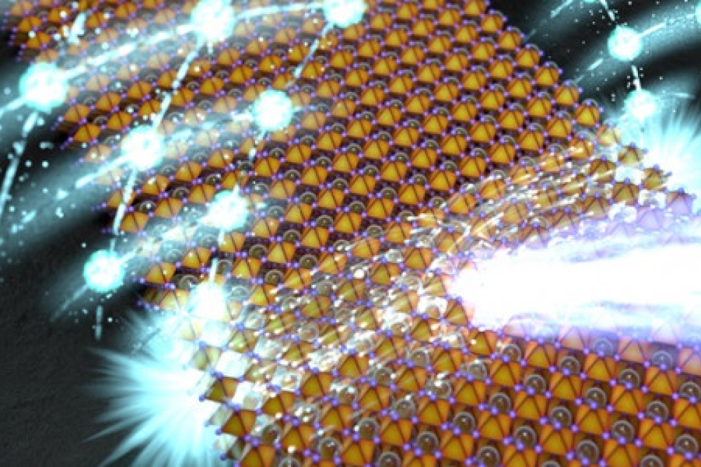
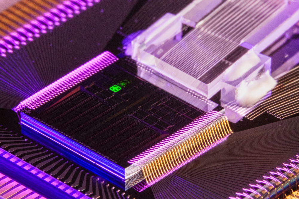
We have a couple of fundamental activities such as continually increasing the complexity of InP monolithic PICs - our most complex chip contains 8 IQ modulators, 2 AWGs, and many other components. In polymer technology, which we are using as platform for hybrid integration, we incorporate, amongst others, graphene into the waveguide for modulation and receiving. This could eventually lead to an Active Optical Printed Circuit Board, where the complete optics is hidden from the surface.
On the more applied side, we develop simple schemes for getting light into and out of PICs -- for example, to be used in silicon waveguide based disposable sensors -- and we continuously decrease the energy consumption of our communication PICs. We also work on first integrated THz emitters.
In addition, we are increasing our efforts in developing generic-foundry platforms that allow partners to design and acquire PICs at relatively low-cost and short time frame. The advantage of having a generic integration platform is that the fabrication process is already there and the partner only needs to care about the design of the PIC.
We expect that many universities, research institutes, and companies, will find this generic-foundry approach attractive for prototyping PICs for their particular application. In fact, the InP platform which has been essentially developed in the framework of the EU projects EuroPIC and PARADIGM is now being offered on a semi-commercial-foundry basis with a run-schedule that takes place four times a year.
How can developers find out more about the facilities and expertise available at the institute? And what are the options for teaming up on future projects?
Our website gives a general overview of our capabilities, although we cannot always share the latest state of research. Within HHI, Martin Moehrle is responsible for the InP platform, and Norbert Keil for the polymer platform. Both have more than ten years of experience in collaborating with industry and academic partners.
As HHI, in accordance with its Fraunhofer nature, focuses very much on applied research, we are also very interested in getting in contact with more fundamental researchers - helping them to evaluate the application potential of their ideas, and to explore the possibly of joint projects.
We would also like to collaborate with all PIC vendors, even when competing with HHI, to highlight synergies and spread the word about PIC capabilities. Whilst telecom and datacom developers nowadays are pretty aware of PICs and their potential, I believe that the sensor or medical, or other related communities are still quite unaware of PIC capabilities. Here, the PIC community should spend much more effort on outreach and education in an easy to understand form, maybe based on existing structures like JEPPIX or EPIC, and existing H2020 Coordination-And-Support-Actions like PICS4ALL and RESPICESME, targeting outreach to SMEs in non-telecom sectors.


