On-chip light sources for ultimately integrated silicon photonics
Ségolène Olivier, an R&D project leader on advanced silicon photonics components at Leti, reviews some of the latest platform enhancements towards more compact, high-performance and power-efficient PICs for telecom networks and data centre applications.
Since the 1990s, from the first submarine optical cable to fibre-to-home deployment and the multiplication of mega data centres, light has become the ultimate medium for high-speed optical communications. Indeed, optical interconnects are progressively replacing their electrical counterparts for shorter and shorter distances.
With the huge increase in data transfer and the number of networked devices, data traffic has exploded in the past decade to reach the zettabyte range, meaning that several billion terabytes of data are exchanged each year. Moreover, this amount is expected to double every two years. This huge traffic explosion creates an unprecedented challenge for both telecom and data centre networks to manage.
Telecom networks require high-performance complex technologies optimized for high spectral efficiency and high bandwidth, due to the cost of deploying the equipment. Data centres, often featuring tens of thousands of servers, will need high-volume, cost-effective and low-power-consumption solutions to connect an extremely large number of ports with a lot of flexibility to allocate jobs to any server at any time. Both telecom and datacom networks will require optical transceivers that combine higher performance with smaller form factors, raising the need for high-level chip integration rather than for discrete components.
Silicon photonics: technology
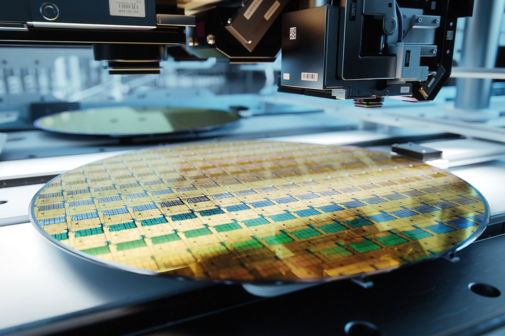
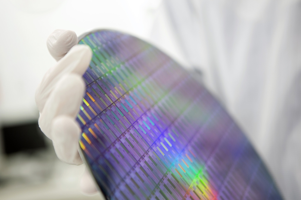
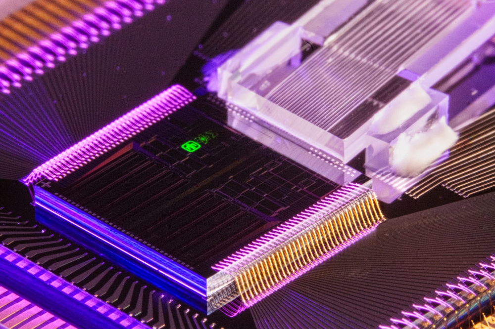
Silicon photonics on a silicon-on-insulator (SOI) platform has emerged as the most promising platform to offer high-volume, low-cost and high-speed interconnect solutions. Leveraging the fabrication infrastructure and processes of the CMOS industry, silicon photonics offers the possibility to integrate a high number of optical functions, such as passives, modulators and photodetectors, operating at high date rate on a single chip. The operation speed can be further increased by implementing wavelength-division multiplexing (WDM) and advanced modulation formats, making silicon photonics technology scalable for a Tb/s aggregated data rate. In addition, silicon photonics integrated circuits naturally lend themselves to 3D integration with their driving CMOS electronics for high-performance, low-cost and small form-factor transceiver modules.
A schematic of a multi-channel transceiver is shown in Figure 1. On the transmitter side, several lasers at different wavelengths with controlled polarization are coupled to several on-chip modulators with their driving electronics. The different wavelengths are gathered into a single waveguide by a multiplexer and then sent to an optical fibre by means of a single polarization grating coupler. On the receiver side, light with arbitrary polarization is coupled from the fibre to the silicon photonic circuit thanks to a polarization-splitting grating coupler, and then sent to a de-multiplexer. This component separates the different wavelengths to different waveguides and photodetectors connected to their electronics, which converts the generated photocurrent to usable voltage. A full library of high-performance silicon photonics components has been developed worldwide to operate at a speed of 25 to 50 Gb/s to build such WDM optical links. Silicon modulators are based on the plasma dispersion effect, in which the charge variation induced by an applied voltage in a PIN, PN or MOS junction is converted to intensity modulation in a Mach-Zehnder interferometer or resonant ring structure, while photodetectors are based on a germanium PIN-junction integrated on silicon.
Silicon photonics: commercial products
Silicon photonics therefore offers a very attractive scalable platform to fulfill the demand of next-generation telecom and datacom interconnects. Complex photonic circuitry can be built to transmit and to detect advanced modulation formats such as polarization diversity multiplexing quadrature phase-shift keying (PDM-QPSK) for coherent transmission. This advanced modulation format, using both multiple phase levels and polarizations of the light wave to code the binary signal, is expected to be used in metro networks and inter-data-centre links. It allows systems to reach data rates of 100 Gb/s per wavelength with hardware bandwidth of 25 GHz and an assembly process far easier than existing technologies combining discrete parts. Such silicon photonics-based coherent transceivers are already commercialized (Acacia Communications).
Figure 1: Schematics of a WDM transceiver with microscopy pictures of the different building blocks fabricated on the Leti 200 mm R&D SOI platform.
A second advantage of silicon photonics is the possibility to manage links in the kilometric range to connect switches in data centres using WDM. This extends the aggregated bandwidth and reach of today's optical links in data centres, which rely on VCSEL-based transmitters and intrinsically limited multimode fibres. As a result, several commercial products for data centre applications have recently emerged, with a data rate of 100 Gb/s per module, such as 100G LR4 CPAK (Cisco), 100G QSFP28 (Mellanox Technologies) and 100G CWDM4 QSFP28 (Intel).
Thanks to the scalability potential of silicon photonics, terabit-class modules are expected in the near future, following the roadmap for Internet switches, with bandwidth density as high as 40 Gbps/cm2 and reduced power consumption. However, until now, the laser source has remained separated from the rest of the chip, leading to high-cost, high packaging complexity and unavoidable coupling losses to the rest of the circuit, limiting the reduction of power consumption. The use of external lasers is also an impediment for practical scalability to much more complex photonic circuits with a very high number of integrated components.
Hybrid III-V/Si platform for ultimately integrated optical transceivers
The heterogeneous integration of III-V semiconductors with silicon by using direct bonding techniques is a promising short- and medium-term solution. This approach exploits the highly efficient light-emission properties of III-V semiconductor materials, such as compounds based on GaAs and InP, as well as the compact and low-loss photonic circuits on silicon.
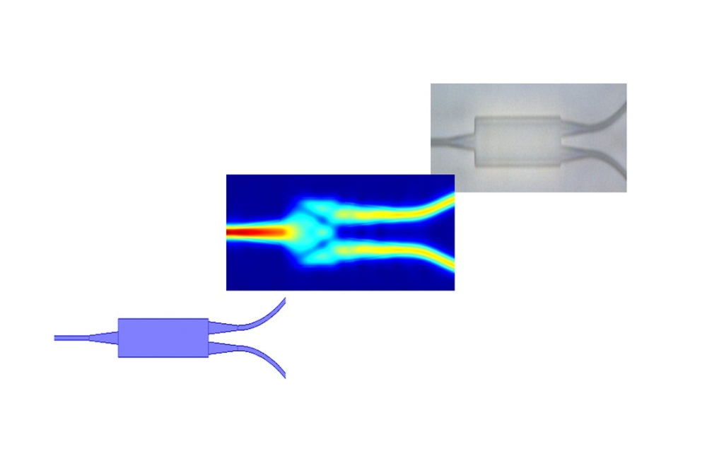
The architecture of a hybrid III-V-on-silicon laser is illustrated in Figure 2. Light is generated in the III-V material, which acts as a very efficient gain medium and is then coupled down through the SiO2 spacing layer to the silicon circuitry. All the elements of the laser cavity, except the gain medium, are fabricated in silicon, which enables higher performance thanks to the maturity of silicon fabrication processes, namely the cavity mirrors "“ for example, Bragg mirrors or distributed feedback (DFB) gratings "“ and additional filtering elements. Fibre couplers are also fabricated in silicon for light output of the lasers. The challenge for such hybrid lasers is to efficiently couple light from the III-V material to the silicon. For this purpose, adiabatic coupling schemes with optimized waveguide shapes have been developed, as illustrated in Figure 2.
Figure 2: Architecture of a hybrid III-V/Si laser with a close-up view of the adiabatic taper in the silicon waveguide to couple light from the III-V material to the silicon integrated circuit.
Leti has developed this hybrid III-V/Si platform using a direct-bonding technique. In this approach, illustrated in Figure 3, unstructured InP wafers or dies are bonded with relaxed alignment tolerances, epitaxial layers down, on a SOI wafer containing waveguide circuits. Afterwards, the InP growth substrate is removed and the III-V epitaxial film is processed by a succession of photolithography, etching and deposition steps.
This integration of lasers on silicon for various communication applications in collaboration with III-V Lab and in the framework of the French IRT Nanoelec project has produced noteworthy results. In the following section, we present some of our recent advances on laser performance improvement and on the integration of lasers with other silicon photonic elements such as modulators.
Hybrid III-V/Si tunable lasers for metro and access networks
High-power tunable lasers are required for telecom applications at 1550 nm wavelength using dense wavelength division multiplexing (DWDM). The laser developed by Leti and III-V Lab and illustrated in Figure 4 (left) is comprised of a hybrid III-V on Si gain section, of Si back and front distributed Bragg reflector (DBR) mirrors to form the laser cavity, a filtering system of two ring resonators within the cavity and a fibre grating coupler at the output. The two ring resonators have a slightly different radius to exploit the Vernier effect to ensure a single-mode behavior of the laser over the whole gain spectral range. Thanks to metallic heaters integrated on top of the ring resonators, tunability over a wide wavelength range of 40 nm has been achieved, together with an excellent monomode behavior and a power level of several dBm, close to that of bulk InP lasers. Compared to discrete bulk InP lasers, such hybrid lasers lend themselves to a higher degree of integration with wavelength lockers or chirp-management components, for example. Direct modulation of these tunable lasers has been demonstrated at 10 and 25 Gb/s, which also makes them excellent candidates for access networks.
Figure 3: Hybrid III-V-on-silicon technology based on direct bonding.
Integrated hybrid III-V/Si laser and modulator at 25 Gb/s
Hybrid III-V-on-silicon lasers have also been successfully integrated with silicon Mach-Zehnder modulators for data centre applications at 1310 nm wavelength. Our integrated single-channel transmitter developed within the IRT Nanoelec project and pictured in Figure 4 (right) has been demonstrated at 25 Gb/s operation speed over a distance of 10 km. The hybrid III-V-on-silicon integration technology also offers new options for modulation and detection. Indeed, other active devices such as electro-absorption modulators, photodiodes and light amplifiers also have been realized. Following this approach, a transmitter based on the integration of a hybrid DFB laser, a III-V/Si hybrid electro-absorption modulator and a hybrid III-V/Si semiconductor optical amplifier were demonstrated at 32 Gb/s operation speed.
Beyond this demonstration, one of the attractive features of heterogeneous integration using III-V dies is the wide choice of gain materials, allowing separate optimization of lasers, III-V electro-absorption modulators and photodiodes to build high-performance, high-speed and low-power-consumption transmitter circuits.
Compatibility with CMOS industrial foundry
The two examples presented above illustrate the exceptional performance of hybrid III-V-on-silicon lasers for fully integrated circuits. Their technological integration scheme can be adapted to extend the compatibility of hybrid lasers with industrial silicon-photonics fabrication lines of photonic integrated circuits, including passive and active devices with several standard front-side metal interconnect levels.
Figure 4: (Left) Hybrid III-V/Si tunable laser architecture. (Right) Optical microscopy picture of an integrated transmitter at 25 Gb/s based on a hybrid III-V/Si laser and silicon Mach-Zehnder modulator.
Leti has developed for the first time a back-side integration process on SOI wafers (Figure 5), compatible with existing silicon photonics fabrication flow at STMicroelectronics's Crolles facility and compatible with electronic-photonic integration on the front side.
Conclusion and outlook
Laser integration in silicon photonic integrated circuits is key for reducing both power consumption and cost and to derive the benefits of the full scalability potential of silicon photonics technology to build complex photonic circuits for next-generation metro and access networks, data centres, high-performance computers and optical networks-on-chip connecting different processor cores.
Figure 5: Schematic of back side III-V/Si integration scheme compatible with industrial silicon photonics SOI wafers, including passive and active devices with standard four-metal level interconnects.
The introduction of new materials in the silicon photonics platform will improve its performance and its flexibility, opening it to a wider variety of applications. Introducing a silicon nitride optical layer, whose refractive index is much less sensitive to temperature than silicon, is another example of silicon photonics platform enhancement. This property can be exploited to build nearly thermally insensitive wavelength multiplexers (MUX) required for low-cost coarse wavelength division multiplexing (CWDM) applications, in which the photonic integrated circuit will remain uncooled. A third example is the hybrid integration of GaAs-based compounds to build non-linear optical devices, such as multiple frequency-combs, paving the way for petabit/s data traffic.
Beyond optical interconnect applications, new areas will be explored such as sensors for the Internet of Things, imagers for augmented reality and bio-photonics for healthcare. These new applications of silicon photonics will require integration of new optical functions with new materials.


