InP lasers: Trumping the incumbents with quantum dots
Very high data rates and tremendous temperature stability make the InP quantum dot laser a very promising contender for tomorrow's optical networks. Johann Peter Reithmaier from University of Kassel and Gadi Eisenstein from Technion report on recent progress in the lab and share their results with PIC International's sister title - Compound Semiconductor magazine.
The semiconductor laser is netting annual sales of billions of dollars, thanks to its deployment in an ever growing number of applications that include optical communication, material processing, medical applications and sensing technologies.
Since the 1980s, sitting at the very heart of this device has been the quantum well. This replaced the bulk material employed beforehand, delivering hikes in reliability and performance. Improvements resulted from the utilisation of a degree of quantum size effects to tailor carrier confinement and tune emission wavelength.
One should not think, however, that the quantum well active region is ideal. It suffers from severe intrinsic problems, and is a far from perfect gain material. Flaws include a laser performance that is strongly dependent on the device's operation temperature, due to the occupation of carriers in states that fail to contribute to laser oscillation. This non-efficient use of carriers makes the threshold current density much higher than one would want it to be. Making matters worse, this limitation is exacerbated with InP based materials emitting in the 1.3 - 1.6 mm range, which is the most important wavelength domain for optical fibre communication.
Another drawback of quantum-well gain material is its asymmetric gain profile. This broadens the emission linewidth of CW lasers and increases their frequency chirp under modulation. If the well could be replaced with a superior gain material that has a symmetric gain profile, emission broadening could be fully suppressed, immediately enabling the fabrication of CW lasers with a narrow linewidth and essentially chirp-free modulation capabilities.
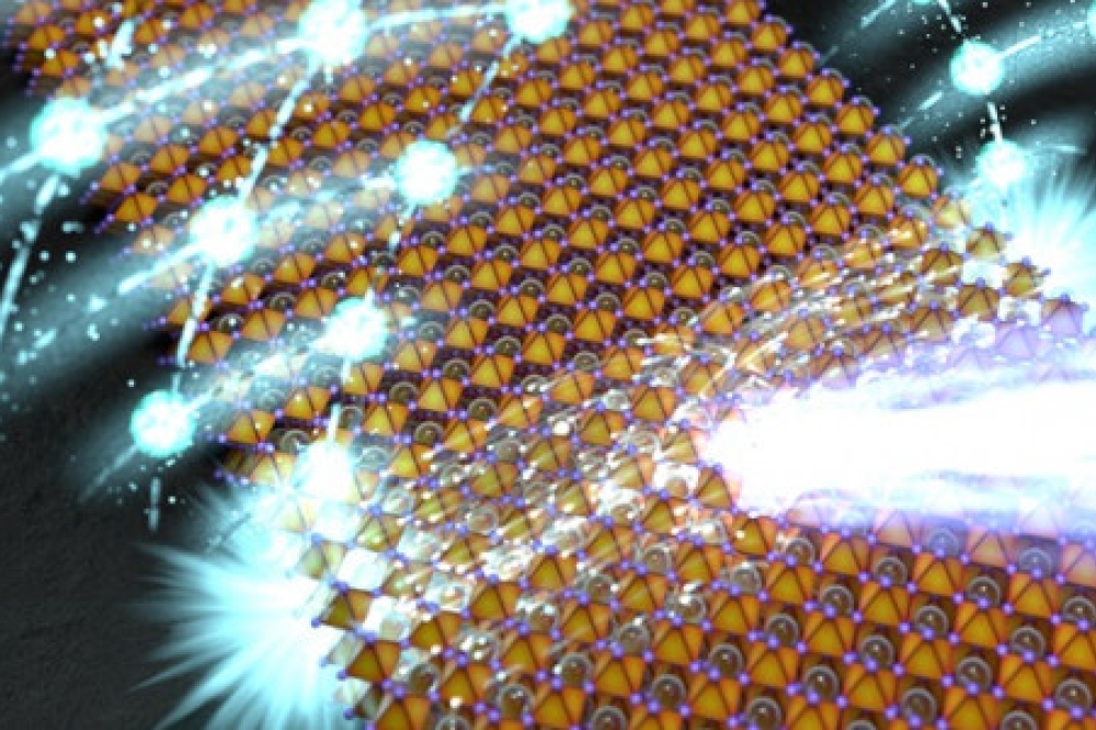
Ideally, an optical gain material is atom-like, with discretized energy levels and occupation restricted to the ground state. To accomplish this, energy separation between the ground state and the excited states must be large enough to prevent the excitement of carriers to these higher energies at any operational temperature. Fulfil this requirement and optical gain will peak at the ground state transition, with no carriers "˜wasted' through the occupation of other levels. Quantum dots that exhibit atom-like behaviour can accomplish this (see Figure 1).
Figure 1. Schematic gain spectra of a quantum well (QW) and quantum dot (QD) material, respectively. The left top picture shows an atomic force microscope image of a high-density QD layer. The figure below illustrates schematically the confined electronic and hole states in a QD and the related ground (E0) and first excited state (E1) transitions. FWHM denotes the full width at half maximum.
The fundamental advantages of atom-like or quasi zero-dimensional gain material are well-established, and were known to developers of semiconductor lasers shortly after the introduction of quantum well materials. However, back then no-one knew how to fabricate a quantum dot laser.
A major breakthrough came in the mid-1990s, through the introduction of the so-called Stranski-Krastanov growth technique. It enables defect-free epitaxy of high-density quantum dot layers (see Figure 1 for an atomic force microscopy image). Unfortunately, the size of the dots within these layers varies, resulting in transition linewidth broadening, due to the quantum size effect. This is a major impediment, because it increases spectral gain significantly. The bottom line is that the predicted intrinsic advantages of ideal quantum dot lasers are masked by the imperfections of nanoscale structures.
In the intervening years, the properties of quantum dot material have vastly improved. 1.3 mm GaAs quantum dot lasers were first produced at the start of this decade, and more recently our partnership between the Univeristy of Kassel and Technion has extended this technology to longer wavelengths, pioneering InP-based quantum dot lasers that operate at 1.55 mm. This material is actually better than GaAs for making quantum dots lasers, as the built in strain is just 3.2 percent, rather than 7.2 percent. This makes InP-based quantum dot lasers mechanically much more robust, and it is also possible to compensate for the compressively strained quantum dot layers with tensile-strained barriers.
Superior temperature stability
Our success hinges on two major breakthroughs in InP-based quantum dot material. Firstly, we have trimmed size fluctuations. This has led to an emission linewidth for a single quantum dot layer of just 17 meV at 10 K, and a corresponding value of 30 meV for a six-layer stack used as the gain region in laser structures. Secondly, we have increased the density
of dots to 6 x 1010 cm-2.
Figure 2. Light output characteristics of pulsed (left) and CW (right) operated short-cavity ridge waveguide quantum dot lasers for different operation temperatures. The back facets are high-reflection (HR) coated, the front facets are as-cleaved.
These advances have had a strong impact on the modal gain of this class of device "“ our laser has produced record values of up to 14 cm-1 per dot layer, or more than 80 cm-1 for an entire structure. So high are these values that they prevent gain saturation, even in the very short laser cavities needed for high-speed devices. Another attribute is that the splitting energy in the dots is high enough to slash carrier losses that come from thermal excitation (see Figure 1).
Thanks to these superb material properties, our lasers have a far higher temperature stability than their quantum well predecessers. Operating in pulsed current mode to avoid parasitic heating effects, ridge waveguide lasers that feature eight quantum dot layers have a characteristic temperature (T0) of 136 K up to 75 °C, and 110 K up to 150 °C (see Figure 2, left).
This figure of merit, which characterizes the temperature dependence of the threshold current, exceeds that of a typical quantum well laser by factors of two to two-and-a-half. Over operating temperatures that span 20 °C to 100 °C, the external differential efficiency "“ that is, the slope of the curves "“ is essentially constant.
We have also characterised the CW output of our quantum dot lasers (see Figure 2, right). Devices with a short-cavity ridge waveguide and six quantum dot layers produce an output in excess of 35 mW at 20 °C, but are restricted to below 20 mW at 70 °C.
Our lasers have been dynamically characterized in small- and large-signal modulation. Plots of small-signal -3dB bandwidth as a function of operating temperature reveal high temperature stability of the modulation bandwidth, which is 14±1 GHz between 15 °C and 60 °C (see Figure 3). The high degree of stability stems from the high temperature stability in threshold current and the consistency in the slope of light output characteristics.
Figure 3. Small signal modulation bandwidth as a function of temperature with nearly constant small signal modulation response between 10 °C and 60 °C. The inset shows an eye-diagram for 30 Gbit/s direct digital modulation.
Eye diagrams for this laser have been obtained under digital modulation (an example at 30 GBit/s is shown in the inset of Figure 3). The eye closes at 36 GBit/s, which is a record for any quantum dot laser.
Manufacturers of high-volume, high-performance components for data-com applications spanning 1.25 - 1.65 mm will take note of this record value, because it demonstrates that our lasers can fulfil the demand for 25 or 28 GBit/s directly modulated data channels without temperature control. Freedom from temperature control and operation at elevated temperatures are highly valued, because they enable our devices to be deployed in low-cost, small form-factor optical cables using course wavelength division multiplexing or simple multi-wavelength pulse amplitude modulation (PAM4) formats.
Encouragingly, the best is still to come for our quantum dot lasers, because they have the potential for even high temperature stability and far faster modulation speeds. Through optimization of the epitaxy and laser design, inhomogeneous gain broadening should reduce, improving spectral gain by a factor of three to four. In turn, the higher gain should lead to doubling of the modulation bandwidth, so that direct modulation rates exceed 60 Gbit/s. Temperature stability should also improve, thanks to a narrowing of the gain peak and an increase in the energy splitting to the excited states.
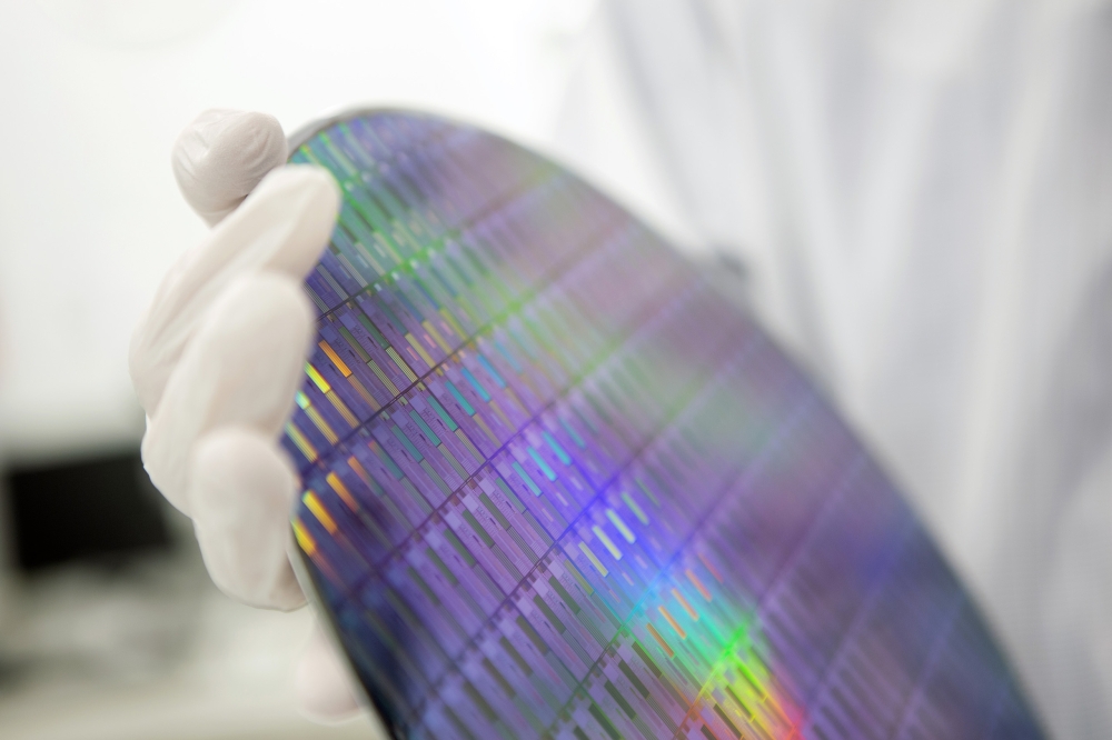
Figure 4. Examples of 3-inch wafer bonding on a silicon-wafer (left) and of die bonding (right) [Courtesy of III-V Lab].
Uniting with silicon
To realise high-volume production, we must combine our technology with that of silicon, so that these devices are manufactured on high-yield, large-wafer fabrication facilities that are already used in silicon photonics. Up until now, the most common approach for hybrid integration of III-V components involves the construction of individual devices using flip-chip technology. However, die and wafer-bonding techniques are under development for devices with more complex functionalities, such as multi-channel transmitters. An example of this approach has been undertaken in the European project SEQUOIA, which includes members of our team at the University of Kassel. Part of this programme involves the development of bonding processes for GaAs- and InP-based quantum dot laser materials on silicon photonic chips (see Figure 4 for an example of wafer and die bonding).
One of the goals for SEQUOIA is to demonstrate data-com transmitter chips for 400 Gbit/s point-to-point communication. Efforts will involve two approaches: 16 directly modulated 25 Gbit/s channels, and a quantum dot, laser-based frequency comb with a 16 channel on-chip ring modulator array. On-chip integration will be with either silicon-based photonic circuits, or together with driver or logic circuits. Regardless of the approach, it is imperative that the process yields a highly reliable, temperature-insensitive, high-performance light source. Our latest quantum dot laser material is better suited to fulfilling those demands than its quantum well counterparts.
Narrow linewidths
As previously mentioned, one of the merits of atom-like gain material is its symmetric gain function (see Figure 1). Ideally, this results in emission with an incredibly narrow linewidth, which can be quantified by a Henry linewidth enhancement factor, a, of zero. In comparison, the value of a in a standard quantum well laser is 3-4, which broadens the linewidth by about an order of magnitude. This indicates that while the linewidth of a III-V laser depends on features of its design "“ such as the cavity length, coupling strength of feedback gratings and quality factor of the cavity "“ it can be trimmed by an order of magnitude by substituting a quantum well active region with an appropriate quantum dot structure.
Figure 5. Emission linewidth of a quantum dot, distributed feedback laser as a function of the injection current. The inset shows the light output characteristics in CW operation and the side-mode suppression ratio (SMSR).
Measurements on our 1.2 mm-long distributed feedback lasers with two quantum dot layers show that as injection current increases to 200 mA, photon density in the cavity rises and linewidth falls to about 110 kHz (see Figure 5). This laser, which has lateral index gratings on both sides of its ridge waveguide, can produce an output power exceeding 9 mW, and realise a stable side-mode suppression ratio of more than 40 dB.
The narrow linewidth above 200 mA makes this laser an attractive candidate for higher order modulation formats in coherent communication, such as quadrature phase shift keying or quadrature amplitude modulation (QAM). With these technologies, the number of detectable symbols depends on the frequency resolution of the reference laser. In high-capacitance transmission lines, modulation formats up to 256 QAM are used "“ they must distinguish 256 states and allow parallel transmission of 8 bits per channel. Further increases in the data transmission rate can come from the Baud rate and the number of wavelengths used in a dense wavelength division multiplexed system. However, for the latter, the reference laser must to be precisely tuned to each channel wavelength, which needs a widely tuneable, spectrally pure light source.
Working within the European EUREKA project SASER, we developed a quantum dot laser that is based on a tuneable light source and utilises the intrinsic quantum features of this zero-dimensional gain material. Our integrated optoelectronic light source contains a distributed feedback laser array with different grating periods (see Figure 6). Applying thermal tuning to this chip "“ that features a quantum dot semiconductor amplifier section to equalise the power levels before boosting them higher "“ allows emission to cover the entire C+ communication band between 1525 and 1570 nm (see Figure 7). Following amplification, the emission linewidth is about 130 kHz, with a value that depends on the laser current, but is independent on the SOA current.
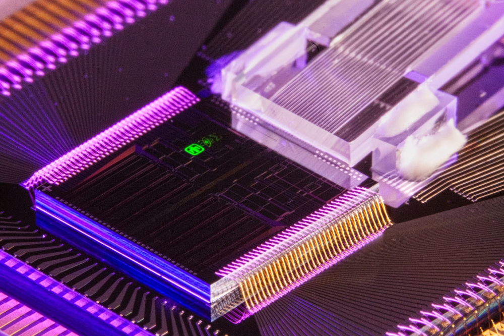
Figure 6. An integrated optoelectronic chip with four arrayed QD DFB lasers, integrated micro-heaters, 3dB coupling network and a subsequent amplifier section. The total chip length is about 4 mm.
Given the complexity of this chip, which is still in its infancy, it is not surprising that it suffers from many imperfections, including high losses in the coupling region. However, it demonstrates the potential of our quantum dot material, which can accomplish a reduction in emission linewidth compared to quantum well gain material without being fundamentally restricted in chip design or laser performance.
The upshot of all our success during the last few years is that quantum dot lasers are now competing with quantum well incumbents in many key areas, while exceeding them in others. Our lasers are comparable to quantum well designs in terms of threshold current density, external differential quantum efficiency, modal gain and output power; and thanks to the atom-like gain material, they have the upper hand in temperature stability, dynamical properties, noise and linewidth.
Armed with all these attributes, InP-based quantum dot laser material seems to be the leading candidate for wafer or die bond processing in hybrid integrated silicon-photonics technology, in particular in regard to reliability issues.
Figure 7. Emission spectra of the laser covers more than the C+ communication band. Each colour shows the operation of one DFB laser out of the four. The wavelength tuning is done by temperature control, either with micro-heaters or the operation current itself.


