Q&A: reflecting on PIC manufacturing solutions
The emergence of advanced modulation techniques in optical transmission provided the perfect opportunity for HHI to strengthen work on InP PICs, as Norbert Grote "“ former deputy director of the organization's photonic components department and now a senior adviser"“ explains.
Monolithic photonic integrated circuits (PIC) have been on the agenda at the Berlin, Germany, based Heinrich-Hertz Institute (HHI) since the early 1980s "“ admittedly a rather ambitious undertaking in those early days of photonics. Some ten years later, PICs could be realized featuring quite a remarkable level of complexity at that time. In particular, a fully integrated heterodyne receiver chip with polarization-diversity architecture was developed comprising 16 optical and electrical elements in total, including balanced waveguide-integrated photodiodes together with field effect transistors for first electrical amplification, a tunable local oscillator BH-DBR type laser, and optical waveguide based couplers, as well as polarization rotator and splitter devices [1]. The emergence of advanced modulation techniques in optical transmission was the perfect opportunity for HHI to strengthen work on InP PICs in the mid of the past decade.
HHI's transmitter and receiver PICs for advanced modulation formats
Since then both transmitter and receiver PICs for phase-modulation transmission schemes have been under development, and as a result several designs are now successfully deployed in commercial products or are at the design-in and qualification stage.
On the transmitter side Mach-Zehnder modulator (MZM) based devices have been extensively developed and applied to a range of amplitude/phase modulation formats like OOK, PSK, QPSK, and 16-QAM. The MZM, the core element for providing high-speed, chirp-free, and spectrally broadband (C-band) modulation, features an active capacitively loaded push-pull traveling-wave electrode (TWE) section along with two MMI couplers and spot-size converters for tolerant optical fiber-chip coupling. Each MZM arm integrates a phase electrode to enable adjusting the operation point of the MZ independently of the TWE reverse bias voltage. The switching voltage is in the range of 2 V, and the extinction ratio above 25 dB. Modulation bandwidth up to ~70 GHz has been achieved. Based on this fundamental device, Inverse Quadrature (IQ) modulator PICs consisting of two nested MZMs have been implemented for single and dual-polarization operation. Monitor photodiodes have been incorporated for facilitating setting of the operation points. The integration of both single MZM and IQ MZM with a BH type DFB laser was accomplished as well. A largely extended multichannel PIC design has been implemented recently targeting coherent optical orthogonal frequency division multiplexing (OFDM) and Nyquist wavelength division multiplexing (N-WDM). The complex PIC shown in Fig. 1, an outcome of the European project ASTRON [2] has an impressive footprint of 15 x 28 mm2 [3].
Figure 1. Schematic and chip image of an 8-channel InP-based all-optical transmitter PIC for OFDM/Nyquist WDM based transmission systems. Coherent optical orthogonal frequency division multiplexing (OFDM) and Nyquist wavelength division multiplexing (N-WDM) are regarded as promising transmission technologies in future flexible optical networks to generate spectrally efficient superchannels with data rates up to several Tb/s. To this end first monolithic InP-based all-optical 8-channel OFDM transmitter photonic integrated circuits have been developed and fabricated at Fraunhofer HHI in the framework of the EU funded project ASTRON [2]. The presented PIC has been designed for an aggregate data capacity of up to 1Tb/s and integrates 180 optical and electrical functions on a chip area of 15 x 28 mm2. This includes eight travelling-wave-electrode type Mach-Zehnder IQ modulators with integrated 50-Ω thin film termination resistors, a specific 8x8 arrayed waveguide grating (AWG) to achieve optical Fourier transform and signal multiplexing, and a 1x8 optical splitter/combiner as the main building blocks. The electro-optical 3-dB bandwidths of the integrated modulators are in the range of 33 ± 3 GHz [3].
Different variants of corresponding coherent receiver PICs have been developed and used in conjunction with single and dual-polarization QPSK and QAM modulation formats. Essentially those chips consist of multimode interference (MMI) coupler-based 90° hybrids, high-speed waveguide-integrated photodiodes, and an optical input spot-size converter at the input. In addition, variable optical attenuators in the form of a thermally tunable Mach-Zehnder interferometer have been incorporated in the signal path for providing intensity control [4]. The most recent design has managed a symbol rate of 100 GBaud [5]. This has been rendered possible by using improved photodiode structures featuring an optoelectronic bandwidth of 90 GHz along with a responsivity of around 0.5 A/W at 1550 nm wavelength. Due to the polarization independent design of the 90°-hybrid intra-symbol phase errors of less than + 5 ° have been achieved over the entire C-band. The latter receiver chip measures only 3.5 mm2 in size.
Integrated ultra-high speed electro-absorption modulated transmitters
Traditional amplitude modulation is yet the easiest way for data generation. And for this, transmitters relying on electro-absorption modulators (EAM) integrated with DFB laser diodes are particularly attractive because of their ultra-high speed and low-chirp potential. At HHI, electro-absorption modulated lasers (EML) have been developed for quite a few years using a fairly simple design in that both the laser and the modulator share the same layer structure. Electrical isolation of both parts is accomplished by an etched trench. In fact, apart from this step the entire EML fabrication is almost identical to that of an ordinary DFB laser. To date up to 70 Gb/s direct modulation has been demonstrated on such components, and accessibility of 100 Gb/s is foreseeable. A drawback of EMLs compared to DFB lasers is the moderate optical output power. To overcome this limitation the structure was extended recently by additionally integrating an optical amplifier section in the same manner as done with the EAM section. 10 dBm of optical output power has been achieved in this way even at a bit rate of 56 Gb/s. And finally, a 4-channel array consisting of such EML structures has been realized that in total is capable of delivering more than 200 Gb/s from a single chip of an area of just 1.8 mm2 (Fig. 2, [6]). Such components are regarded as highly attractive for data centres, even if this booming application field is commonly believed to be the realm of Si-photonics.
Figure 2. 4-channel array of 56 Gb/s electro-absorption modulated DFB lasers (EML). Each EML in the array consists of three different integrated elements: DFB laser diode, electro-absorption modulator (EAM), and an optical amplifier (SOA) to boost the output power. All of them rely on the same structure, including an InGaAlAs MQW active region, which not only largely eases fabrication but also ensures low-loss optical coupling and negligible optical reflections between the different sections. To ensure transparency of the modulator in the on-state the DFB wavelength is shifted towards the long-wavelength side of the gain spectrum by design. In the presented array each EML exhibits a different emission wavelength (~1569 "“ 1577 nm range) with a spacing of 2.5 nm. All devices are electrically accessible from the back side. The 4-EML array measures 2.5 mm x 0.7 mm. Each individual EML is capable of 56 Gb/s modulation enabling generation of a total bit rate of 224 Gb/s from the 4-array component. No noticeable interference on bit-error-rate behavior was found when simultaneously operating adjacent EMLs. Typical peak-peak modulation voltage amounts to 2 Vpp around a bias voltage in the 1.1-1.4 V range [6]. The EML transmitter array can be used in space division multiplexing mode with four separate fibers (PSM4) or for wavelength division multiplexing schemes (WDM).
Generic PIC platform
The PIC implementations outlined above are relying on dedicated designs and technology for optimized performance. For photonic integrated circuits to become more widely deployed in diverse application sectors, the adoption of a foundry business model in photonics is highly convincing. For this goal InP is unique in that it provides the only materials platform allowing for integration of virtually all optical functionalities required, in particular those needed for light generation and amplification which is not feasible in silicon.
The foundry approach was tackled in the recent EU projects EuroPIC [7] and PARADIGM [8] which were geared towards investigating and establishing the entire eco-system needed for making generic InP photonic integration a reality. Accordingly, the work program encompassed development of integration technology and building blocks; design platform and tools; process design kits (PDK); and (to a lesser extent) generic PIC packaging. The latter task is now extensively being continued in the recently started EU Pilot Line project PIXAPP [9]. Fraunhofer HHI was and is participating in these projects. In EuroPIC & PARADIGM it was mainly engaged with technological platform development and execution of "foundry" wafer runs implementing PIC designs from project-external users.
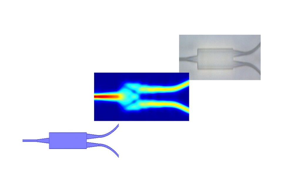
Figure 3. Waveguide-based polarization converter integrated between EAMs. A polarization converter rotating the plane of polarization represents a key optical element for managing polarization in a PIC. On HHI's platform a structure has been adopted that consists of two ridge-waveguide sections with slanted sidewalls. Thanks to a refined design the most critical fabrication tolerance could be significantly relaxed to ~ +/- 10%, compared to previous designs, whilst still allowing for a TE/TM extinction ratio (ER) of 20 dB. Experimental results have so far shown ER levels of 15 dB over the full C-band, and an insertion loss of < 1 dB (TE) [10]. The total device length including transition tapers amounts to some 700 µm. The photograph shows an image of such a polarization converter integrated between two serial electro-optical modulators to enable polarization-multiplexed modulation. [11]
The starting point of HHI's generic platform development was the high-speed waveguide-integrated photodiode structure which has been a key component in HHI's research portfolio since the early 1990's and which, by the way, served as "starter kit" of u2t Photonics (now Finisar Germany GmbH), when founded as a spin-off company of HHI in 1998. This PD structure, including an evanescently coupled waveguide section, represents the main building block for the receiver (Rx) part of the PIC platform. With three different waveguide designs available to support bending radii down to 150 µm, a variety of passive optical building blocks has been introduced, amongst them polarization splitter and converter [10, 11] (Fig. 3) elements for polarization handling. The full capability of InP based photonic integration is achieved by subjoining transmitter-type (Tx) building blocks: mainly gain elements/optical amplifiers; lasers; phase shifter and modulator devices. A schematic of the entire platform [12], referred to as TxRx platform, is depicted in Fig. 4, and Table 1 gives an overview on the currently available building blocks. A crucial feature of HHI's unique platform concept is the use of semi-insulating substrate and waveguide material which favors high-frequency performance and supports electrical isolation and reduction of electrical crosstalk effects.
Figure 4. Schematic layer structure and basic building blocks of HHI's TxRx PIC platform. The generic PIC fabrication process commences with the growth of the base wafer layers (indicated by the white arrow) consisting of a Fe doped InGaAsP/InP waveguide layer stack and the half-structure of a laser ("Tx structure"), all deposited on a semi-insulating InP:Fe substrate. The active region, designed for C-band operation, is formed of an offset multi-quantum well (MQW) stack on top of a quaternary bulk waveguide layer. This stack is used to create laser gain elements, SOAs and electro-absorption modulators (EAM). At places where DFB laser elements are to be positioned 1st-order complex-coupled DFB gratings are formed. In the same way tunable Bragg gratings (BG), a building block for e. g. wavelength tunable DBR lasers or vertical coupling structures, are implemented after locally etching off the MQW material. Without grating, this section can be used for electro-optical phase shifters (PS). The Tx elements are mesa-etched down to the insulating bottom waveguide region thus providing full electrical isolation. These steps are followed by the selective-area growth of the "optical passives & photodiode" layer stack. The same passive waveguide layer interconnects both the photodiode (evanescent coupling) and the Tx devices (butt-jont coupling) and serves for building all of the passive optical elements. The entire wafer fabrication involves only three epitaxial growth steps, including base wafer growth, and about 25 lithographic mask levels. The individual chips are delivered with facet coating according to customers' needs.
Multi-project wafer runs
A distinct advantage of generic platforms is the possibility to execute multi- project wafer (MPW) runs shared by multiple users. HHI has launched MPW runs on a semi-commercial basis in 2014, now scheduling four runs per year. Including the runs performed in previous projects more than 60 different PIC designs from industry and academic groups have been fabricated meanwhile (example shown in Fig. 5). An individual user can choose a minimum design cell of 4x12 mm2, or a multiple thereof, allowing for very affordable prices for prototype chips. PDK implementations are being offered and maintained by a number of established vendors of photonic design & simulation software: PhoeniX BV; Photon Design Ltd.; VPI Photonics GmbH; Filarete S.r.l.; and Lumerical Solutions, Inc. (in progress). MPW runs may be accessed by contacting JePPIX [13] providing brokerage services or HHI directly, and also through the EU-projects ACTPHAST [14] and PICs4ALL [15].
Table 1. Compilation of building blocks (BB) currently offered on HHI's InP integration platform
JePPIX, the prime consortium of European stakeholders in photonic integration, plays a pivotal role in this community. Besides brokering activities it is, amongst others, involved in promoting PIC technology to broaden awareness in the public and professional domain; in developing and maintaining road maps; and not least in organizing PIC training. Through the latter newcomers and advanced learners are educated in not just PIC design, but also made aware of new market opportunities. Such training sessions have been held in JePPIX's "hometown" Eindhoven, The Netherlands, for many years, but have recently been stretched out worldwide, with events organized in Boston (US), New York (US)*; Daejeon (S. Korea); and end of 2016 in Santa Clara (US)* and Beijing (P.R.C) (* principal organizer: 7pennies Consulting).
Figure 5. Example of customer specific PIC made on HHI's MPW platform
To cope with the growing capacity and coverage demand for wireless services the EU-COMANDER project [18] has proposed a Next Generation Network that merges the optical and wireless infrastructures. A key component thereof is a Remote Access Unit. A respective PIC was designed by Bright Photonics BV and fabricated on a MPW run at HHI. The photonic circuit utilizing arrayed waveguide gratings (AWG) as demultiplexer to provide six discrete spectral passbands between 1510 nm and 1570 nm - is intended for Fiber-To-The-Home (FTTH) and Radio-over-Fiber (RoF) services [19]. Further building blocks used in the design are tuneable DBR and DFB laser diodes, SOAs, current-injection tuneable Bragg gratings, high-speed photodiodes and thermo-optic phase shifters. In full operation all signals are processed simultaneously by dedicated tuneable receiver and transmitter sub-circuits.
Active PICs for hybrid integration
Despite the high capabilities of monolithic InP "“ and likewise Si "“ based photonic integration platforms ultimate limitations in performance and complexity may not be ignored. Hybridization of PICs implemented on different classes of materials is considered an efficient way to expand those limits. In Si photonics hybrid (or hetero-) integration of InP-based light sources/ amplifiers is inevitable to achieve full TxRx functionalities.
The combination with dielectric material platforms, made e.g. of SiNx or polymers, is another dimension to create integrated optical components with enhanced performance. Optical chip-to-chip connectivity is the big technological challenge here. To this end, various solutions are being currently explored by many groups. HHI has been pursuing a polymer based hybrid integration platform [16] for many years but is also engaged in other hybrid developments by contributing adapted active InP devices.. In a recent collaboration with IBM-Watson Research Center, HHI has developed InP optical amplifier arrays that were designed for flip-chip mounting into a Si based waveguide network for optical switching (Fig. 6, [17]). A specific requirement was to achieve not only optimal coupling performance but also to make the chip fit in-between the waveguides with high longitudinal precision. The latter was accomplished by adopting etched rather than cleaved facets.
Figure 6. Integrated SOA array for hybrid integration onto Si photonics platform
For photonic switch matrices InP based 4-channel SOA arrays have been developed which were flip-chip mounted onto a Si photonic carrier with SiN waveguides. The SOAs with a 250 µm pitch feature tapered spot-size converters at either end for efficient optical coupling to the SiN waveguides and incorporate appropriate flip-chip assembly structures, including reference stops. The facets, tilted by 7 deg, are formed by dry etching to provide lithographic precision of the length (1 mm) of the SOA devices. Fiber coupling to assembled modules demonstrated >10 dB fiber-to-fiber gain over 60 nm bandwidth centered at 1550 nm for all SOA channels. Each SOA was shown to support error-free 4-wavelength 25 Gb/s WDM links (collaboration IBM/HHI [16])


