Reinforcing the PIC industry global supply chain
Jose Pozo, Director of Technology and Innovation at European Photonics Industry Consortium - EPIC, offers his perspective on what's needed to strengthen each step in the delivery of photonic integrated circuits so that the sector can flourish and reach new heights.
Currently, the supply chain for the delivery of photonic integrated circuits (PICs) is scattered over many companies who are offering a small piece of the chain - for example, chip design, foundry, testing, packaging. Customers who are interested in using PICs in their applications have to manage the interfaces between the different suppliers, which can be very complex and where the ownership of the total functionality is not well defined. Hence, what I believe to be the main challenge of managing the PIC supply chain is to understand and reinforce the weak links and their impact on the full chain operations as well the unexpected disruption they may cause at a site level.
This challenge becomes even more difficult given the interdependency of each of the links - for example, PIC designers need to satisfy end-user specifications using standardised building blocks by the foundries which will be processed initially in multi-project wafer (MPW) runs, fabricating many products for very different applications on the same wafer. These standardised building blocks, which in many cases have been created by the PIC designers, need to satisfy the needs of the packaging facilities. However, the packaging being the interface between the chip and the system, needs to be fitted to a system with very well defined specifications in terms of size, cost, environmental conditions, and which of course also affects the design of the chip.
Bringing it all together
Fragmentation in the supply chain (design, simulation, manufacturing, test, qualification, productisation, industrial-engineering, product development, application focus and PIC capabilities marketing) needs to be solved through bringing all the aspects under one umbrella, with focus on the applications and what the customer really wants, offering a one-stop shop with application engineers that manage the technology and solve the problems through collaborative efforts. However, the fact that very few vertically integrated companies in the PIC arena exist shows that solving this fragmentation issue is not an easy task.
A positive example is the recently created LioniX International, which acquired LioniX, Satrax, XiO Photonics and OctroliX, resulting in a vertically integrated company offering complete customised modules; from chip design to high-volume module assembly. In this way the chip design, packaging and assembly process can be optimally tuned together in order to best meet the customer requirement and providing customised microsystem solutions.
Solving the software and design puzzle
A scarcity of robust photonic design manuals, commonly known as Processed Design Kits or PDKs (including rule checks and calibration of building blocks, compact models for circuit simulation, yield information and capability for statistical performance prediction) categorically limits the expansion of integrated photonics technology into wider applications. In addition, integrated design tools that would seamlessly combine different simulation methods for the component-level, system-level simulations, mask design and fabrication tolerance analysis, do not yet exist. In that sense PIC design is far behind the IC design tools.
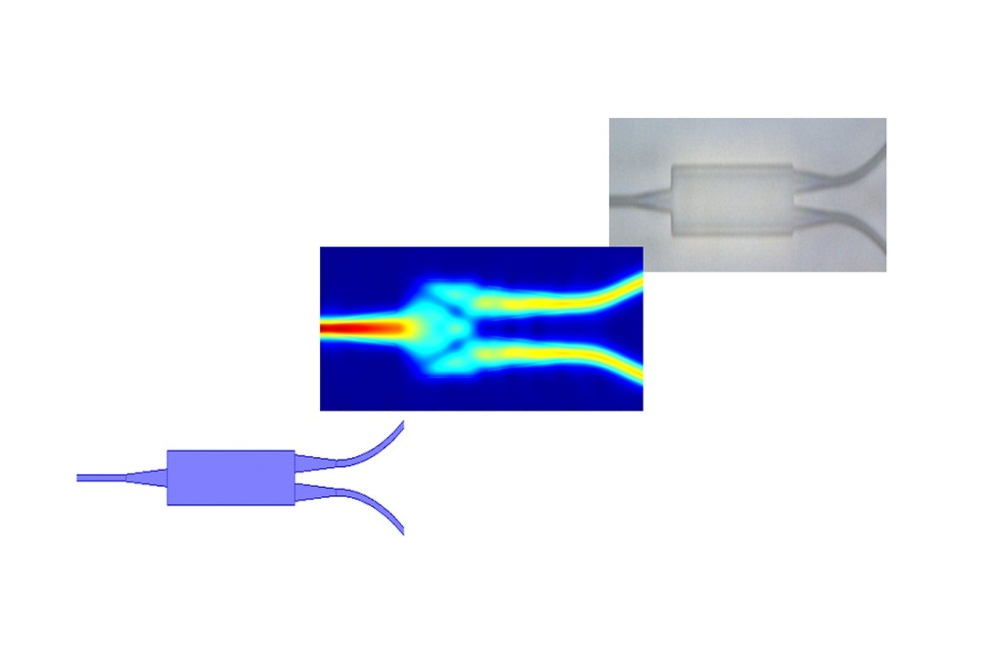
However, the sector is stepping up to the challenge. Lumerical's efforts are a good example of a company addressing exactly this area, as they are one of the few vendors who offer multiple solvers needed to address various aspects of active and passive photonic component and circuit design. This enables Lumerical to collaborate with Electronic Design Automation (EDA) and Photonic Design Automation (PDA) tool developers, such as PhoeniX Software, and to develop highly integrated tool flows that enable the development of the PDKs, and the reliable, scalable design of integrated photonics into PICs or combined electronic/photonic System on Chip (SoC) architectures.
Such PDA tool developers enable easy and cost-effective realisation of integrated photonics chips and systems by means of superior software covering the entire design flow. The established collaboration between PhoeniX, Lumerical and the EDA developers Mentor Graphics and Cadence Design Systems represents a good example of companies finding ways to team up whilst also strengthening the common supply chain. Along a similar line, it is worth mentioning the collaboration between the EDA tool developer and design support provider Luceda Photonics and CST (Computer Simulation Technology AG), which together can provide full-wave photonic simulation of components that is often needed to extract more accurate component models, or to study the effect of heat on the component.
Co-integration challenges
Enabling application/chip level designers to leverage integrated photonics as a tool to address end application and integrate into SoC architectures and more complex PICs composed of hundreds or thousands of elements will allow the market for integrated photonics to expand. This will, in turn, drive wafer starts which are what's really needed to see integrated photonics become a sustainable, viable, cost effective technology offering. A good example of a company leveraging that scenario is Sicoya in Germany. Sicoya's transceiver technology is based on the co-integration of photonic and electronic building blocks on one single chip with a standard CMOS backend. The availability of ultra-small photonic components lets the cost intensive chip real estate be dominated by electronics rather than photonics, which is turning co-integration into a commercially viable fabrication process. The main benefits of this approach are substantial improvements of link budget as well as power efficiency due to higher sensitivity, smaller parasitics and lower driving power. Co-integration allows for greatly reduced packaging complexity.
It is indeed the co-integration of electronics and photonics ICs that still represents numerous challenges for the sector, especially when dealing with broadband communication applications with typical high bit rates. The HNI Institute at the University of Paderborn is helping to addressing these issues by combining nano-meter CMOS, SiGe BiCMOS, silicon photonic technologies.
Seeing the current unbridged gap between technology and application was one of the reasons for VLC Photonics in Spain to make a move in their value chain position. While VLC was well established as an independent PIC design house, they decided to enlarge their service portfolio to a complete solution provider in everything related to photonic integration. Nowadays, they do not only provide services for PIC engineering and optical chip design, but also brokerage for manufacturing at all main technology platforms (+20 foundries) and for packaging through a large network of partners.
Feeding the appetite for growth
As commercial PIC volumes, diversity and complexity show a rapid increase, a point of concern is the present shortage of open-access manufacturing lines for medium and large volumes in the supply chain. Also, in order to sustain the growing appetite for PICs, process control and tooling from design to finished product will have to further mature. The chain needs to better predict yield and performance for lower non-recurring engineering (NRE) and reduced time to market. PIC based products rely in many ways on a new supply chain and the first higher volume applications will have to clear the pipeline. In that respect, Imec offers an open, agile and rich Silicon Photonics platform accessible to any user. The platform supports a wide variety of architectures with best-in-class component performance for most components, enabled by a robust CMOS manufacturing approach. What's more, Imec will extend this approach in the coming years with a SiN platform targeting specifically life science applications using near-IR and visible light.
One the potentially weakest links is the PIC cost for its specific application market (datacom, telecom). On the one hand 80 percent of the cost is due to packaging that is not easily scalable, while on the other hand the market volumes are medium/small leaving the cost at a medium level with a very slow trend to lower values. In addition, many equipment manufacturers are vertically integrated and therefore often either the chip supplier is internal or they have exclusive contracts with specific foundries. The granularisation of suppliers also limits the cost reduction of technology.
In 2012, with the help of the French Government, the 'IRT Nanoelec Silicon Photonics Program' was launched in the Grenoble area, bringing together under one roof the expertise and equipment needed for the development of Silicon Photonics technology and associated solutions for optical communications, and aiming at efficiently transferring the developments to the industry. Mentor Graphics, STMicroelectronics, CNRS and CEA-Leti were the core members of the consortium setting and driving the Silicon Photonics Program. In 2015, a new key partner, Samtec, joined the consortium, bringing strong and complementary skills in optical and high speed electrical packaging. The consortium, headed by CEA-Leti, is now gathering research institutes counted among the pioneers in silicon photonics and major industrial players over the complete value chain (silicon foundry, fab and test equipment, EDA, packaging). For end users, this is a key factor for success for developing innovative solutions.
In addition, it's worth mentioning the remarkable efforts of the Institute of Photonic Integration at TU Eindhoven, the knowledge engine of the Photon Delta ecosystem in the Netherlands, which combine high tech companies leading in PIC, such as the first pure play commercial foundry for InP-based PICs, Smart Photonics, or SoC manufacturer EFFECT Photonics using high-density electrical interconnect and packaging technology. Beyond European borders, the industry is trying to solve the lack of volume in manufacturing. The American Institute for Manufacturing Integrated Photonics (AIM Photonics) is the American answer to the European push of PIC Industry, with these driving forces many advances in the industrial take-up of PICs is expected.
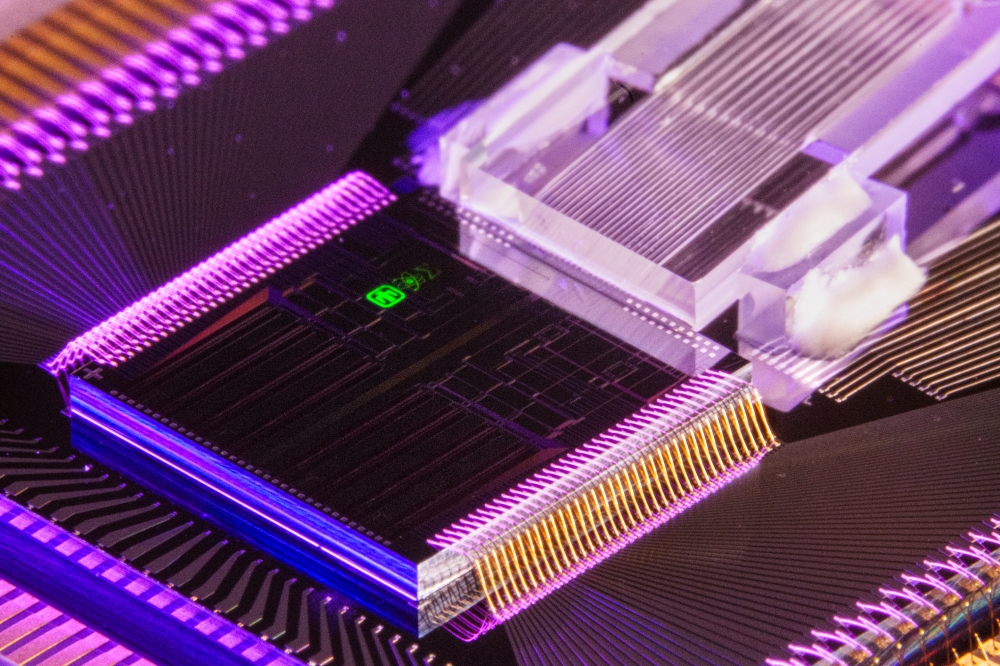
Furthermore, the contributions of the Photonics Electronics Technology Research Association (PETRA in Japan) are also acknowledged. PETRA develops O/E and E/O components based on silicon photonics and unique packaging concept of "Optical I/O Core". This small and high density form-factor with user friendly optical and electrical interface offer building blocks for pluggable optical modules, embedded optical modules, and multi-chip modules of optical I/O chips and electrical LSI.
Figure 1. Optical I/O Core PIC by PETRA.
Perfecting the package
Packaging is one of the most important next steps for the commercialisation and usage of PIC components, and the effort that it takes to perfect a solution is often underestimated. Over the years many new functionalities have been developed on chip, and arrived at a moderate manufacturing readiness level (TRL = 3-5). However, packaging technologies have not necessarily been evolving at the same rate and were awaiting the breakthrough of PIC's and their promised turnover.
INPHOTEC in Italy and Tyndall National Institute in Ireland are providing concepts for the packaging and system conception of PICs, leading to innovative solutions in automated (robotised) packaging, enabling small production and pilot manufacturing lines of assembled PICs. Techniques, such as the active and passive alignment for PIC assembly provided by companies such as ficonTEC and Aifotec, as well as novel process such as 3D printed photonic wire bonds by Nanoscribe, the transfer molding by Advanced Packaging Centre or the alignment of polymer waveguides with submicron tolerance by Vario-optics are established in the market, but not standardised.
Potential users of PIC would very much benefit from some level of standardisation. This standardisation should not target low mass production costs - for a product in mass volume there is enough budget to develop an optimised package. Standardisation should target to reduce the design and manufacturing effort to get the first 10s or 100s of samples. One of the tendencies in order to consolidate new technologies is standardisation as a means to reduce costs and improve efficiency in the supply chain. Generic processing is one of the ambitions for integrated photonics in order to reach this state to some extent. The advantages are obvious: reduced costs and lead-time in the supply of PIC based components for customers. The risks however are current yield expectancies and ongoing development of functional capabilities needs.
A well balanced interaction capability on a technical level between supply chain members (designers, foundries and integrators) is imperative towards touching commercial base in the end. Only sufficient mutual understanding of needs and (potential) capabilities will make things work, which requires a strong collaborative effort from all parties involved. Linkra, in Italy, aims to solve that issue in the supply chain, as it can provide complete system integration (development and production) for third parties in combination with full assistance and technology transfer for setting up their production (assembly instructions, machine settings, operator training).
Let us try to imagine the future of PIC standard packaging processes: Photonic ICs like electronic ICs are first and independent of the technology used in semiconductor chips. They are bonded to a substrate fanning out the electrical chip connections - standard wire bonds. For RF signals additional surface mountable connectors are added to the substrate together with a standardised optical jack. The latter one available in different outlines. All the components on the substrate are covered by a material serving two main purposes. Similarly, for electronic ICs it offers protection of the chip and the wire bonds. However, and this is the part unique to photonic ICs, we do not have an optical interconnect yet between chip and connector jack.
Supporting all stakeholders
One of the weak links from the designer's perspective in PIC technology is a degree of inflexibility in the technology platforms that are offered by foundries - for example, MPW services. Today, the 220 nm SOI platform dominates the silicon photonic MPW services for the telecom wavelengths, but this platform might not be the optimal one. Exploring other, specifically optimised for a variety of applications (telecom, datacom, sensing, including Mid-IR applications), and developing photonic components on these platforms is very interesting to the research community. Current photonic MPW services need to expand to meet this need.
However, from the perspective of wafer market, current demand for PIC devices is relatively low compared to microelectronics and therefore there is little economic sense for suppliers to provide other platforms that are not supported by demand in the microelectronics. This is now becoming a classical chicken and egg problem where foundries are not adopting other platforms due to insufficient demand and the research community is not getting the optimum platforms for applications that could create such a demand and boost production of specific PIC platforms.
Linked to the inflexibility in platforms, MPWs can sometimes hamper device innovation due to the desire to standardise the device designs offered. Often, this does not suit researchers who may wish to try more innovative device and/or photonic circuit designs. To solve that issue, the University of Southampton is launching the Cornerstone MPW service for UK academia (and potentially other customers) where they plan to offer fabrication of PICs on additional SOI platforms to researchers, with some flexibility in device design capability.
Reinforcing the chain
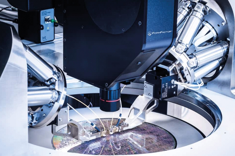
Testing is an essential element in the PIC supply chain and needed at various stages: in-line process monitoring for statistical process control; building block characterisation for PDK enhancement; wafer validation for wafer release (specs compliance); pre-packaging (entry) testing. Testing of PICs in volume needs large investments in automation as well as standardisation of the parameters to be measured and their tolerances. ficonTEC in Germany is positioning itself to solve that issue.
Material matters
At the present stage, photonics comprises a variety of co-existing material platforms. From the well-established Silicon Photonics brokered by Europractice and Indium Phosphide and TripleXÂTM brokered by JePPIX, the Silicon Nitride technology offered by IMB-CNM in Spain, to the incoming manufacturing of PIC on GaAs platform employing the Quantum Dot technology of Innolume in Germany, and many more. All of them have specific strengths and drawbacks. At the moment, there is no platform that can provide all functionalities at once.
To efficiently combine the strengths of the existing platforms, it is important to provide a reliable and scalable PIC technology that enables multi-chip photonic systems, clearing the path to novel system architectures with unprecedented performance. In particular Silicon Photonics for communication has seen major interest providing volume demands for data centres, especially for the short-reach links for datacentres. However, the need for a low cost, easily integrated in volume has been a drawback. This is currently the main obstacle for implementation of Silicon Photonics in datacentres. However, in the most recent years activity on the development of integrated light sources has increased notably.
PICs very often rely on combining III-V materials with silicon to gain the benefits of both worlds. Fraunhofer HHI has made very good efforts in solving that issue, creating an InP-based PIC platform focusing on high quality integrated lasers and SOAs, with a key potential application in combination with Silicon Photonics for data centres. Another good example is the work of VTT, combining PICs with III-V chips and electrical ICs using hybrid integration.
Wider adoption of Silicon Photonics is partly impeded by the dependency on specific fab technologies, due to the small number of high-performance processes that are available worldwide and a lower abstraction level of the PIC design compared to electronics. With the aim to solve the major challenge of multi-platform integration, EVGs extensive know-how in wafer bonding and heterogeneous material integration enables the merging of different material systems very efficiently. Furthermore, with nanoimprint lithography (NIL), EVG provides a patterning technology which perfectly fits to the needs of photonic applications in general. This is also supported by EVG's NILPhotonics® Competence Centre, which was established to jointly overcome challenges and shorten the time to market for innovative products with its customers and partners in the supply chain.
Figure 2. EVG Automated Production Wafer Bonding System
Acknowledgments
EPIC wishes to thank its members and those who contributed their perspectives for this column; they include: Torsten Fiegler (Sicoya), Jonas Flueckiger and Bill De Vries (Lumerical), Dario Lo Cascio and Antonello Vannucci (Linkra), Dan Gale and Dan Deptuck (CMC Microsystems), Ronald Broeke (Bright Photonics), Gunther Vollrath (Aifotec), Liesbet Lagae and Philippe Absil, Amit Khanna (IMEC), Sylvie Menezo, Jean-Mark Fedeli and Vincent Reboud (CEA-Leti), John O'Carroll (Eblana Photonics), Timo Aalto (VTT), Martin Hermatschweiler and Nicole Lindenmann (Nanoscribe), Joost van Kerkhof, Paul van Dijk, Ronald Dekker, Paul van Dijk and Arne Leinse (LioniX International), Martin Eibelhuber and Clemens Schuette (EV Group), Jeroen Duis (TE Connectivity), Tobias Lambert (Vario Optics AG), Norbert Grote and Martin Schell (HHI), Giancarlo Prati (INPHOTEC), Niek Nijenhuis and Twan Korthorst (PhoeniX Software), Rolf Evenblij (Technobis), Joerg Pieter (CSEM), Umberto Rossi (PETRA), Carlos Dominguez (IMB-CNM, CSIC), Alexey Shkolnik and Daniil Livshits (Innolume), Nicole Lindenmann (Nanoscribe), Marco Koelink (APC), Chris Scheytt (HNI, University of Paderborn), Yuqing Jiao, Katarzyna Åawniczuk, Kevin Williams (TU Eindhoven, JePPIX), Iñigo Artundo and David Domenech (VLC Photonics), Guillermo Carpintero (UC3M).
Please note the article only reflects the opinion of the author and not necessarily the views of each of the individual contributors.


