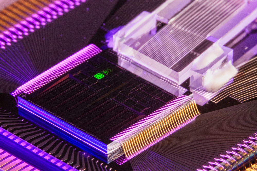
Introducing PLASMOfab: a new era in CMOS-based PIC technology
Surface plasmon polariton (SPP) based designs pave the way for monolithically co-integrating photonics, plasmonics and electronics towards volume manufacturing of high-performance and small-size photonic modules. PLASMOfab's project team reveals the plan for 2016-2019 and highlights future opportunities for upgrading communication in data centers or developing low-cost medical diagnostics, to give just a couple of examples "“ read on for the full story.
Photonic components constitute a major driving force of the European and global economies across a diverse range of technology sectors including ICT, medical, environmental, military and space applications with a total world market estimate of 30 billion Euros. Despite this massive demand, most photonic devices are large and bulky while in some cases they are assembled from discrete components with very little automation. The net result is fragmentation of development efforts, expensive optical devices and, to make things worse, difficulties in effectively aggregating large scale circuits to address more complex functionalities at a low size and cost. To address these market needs, photonic integrated circuit (PIC) technologies are required as the means to realise mass production of photonics as analogous to the production roadmap followed by the electronics industry for chips enclosed in mobile phones, tablets or other commercial electronic appliance.
Merging the paths of electronics and photonics
In fact, the PIC industry will have to take advantage of the currently dominant, best-in-class processes of electronic CMOS manufacturing infrastructures to decrease time-to-market and maximize return on investment. In this context, silicon-related photonics is the integration technology of choice matching the basic CMOS process profiles in one hand and favouring monolithic integration of photonics with supporting electronics on the other, simplifying overall integration and packaging, increasing density and enabling tighter device-to-circuit proximity. However, the significant dimension mismatch between photonic and electronic components hampers the consolidation vision. In reality, photonic devices are large when compared to transistors keeping the fabrication process of each chip separate. To address the rapid manufacturability of complex photonic-electronic ICs in large scales, the development paths followed by electronics and photonics will need to merge.
PLASMOfab was conceived with a clear motivation to address the above set of needs and trends. PLASMOfab is a new ambitious project funded by EU-HORIZON2020 framework, launched on 1st January 2016 with the goal to develop a new PIC technology that leverages plasmonics as the means to bridge the gap between photonics and electronic ICs, addressing the needs for mass-manufacturing of low energy, small size and high performance PICs through mainstream IC fabs.
Guiding light at sub-wavelength scales
In most common Si-based photonic integrated circuits, the waveguide cross-sectional dimensions are below or comparable to the transmitted light wavelength ensuring single mode guiding and a reasonably small mode size. In order to further reduce the photonic mode and stretch PIC functional density, Surface Plasmon Polariton (SPP) based waveguides are deployed. SPP waveguides have attracted intense research efforts in the last decade owing to their unique ability to guide light at sub-wavelength scales, as they make it possible to overcome the diffraction limit of light and confine light into a width of few tens of nanometers due to coupling to electron plasma oscillations near the metal interface. The ability to guide the optical field on the metal surface in a PIC provides unique light-matter interaction properties that may be exploited to enhance sensitivity per unit length in sensing components or increase non-linearities such as Pockel's effect in electro-optic modulators for ultra-high speed data communication applications. Moreover, SPP waveguides provide the advantage of sending both electric and photonic signals along the same circuitry, thus naturally incorporating electrically driven components in plasmonic-augmented PICs.
In this context, PLASMOfab is expected to optimally combine the best of all three worlds of plasmonics, photonics and electronics in a single CMOS compatible integration platform, enabling mass production of PIC-based modules with unprecedented performances and functionalities like eco-friendly terabit communication systems in data centers or disposable multi-sensor chips for single molecule detection in medical diagnosis (figure 1).
Figure 1: The approach of PLASMOfab: Develop and standardise plasmonic components and interfaces with photonics and electronics. Synthesize plasmonic, photonic and electronic components in CMOS wafer-level fabrication to demonstrate low cost, mass fabrication of high-performance photonic modules in two predominant industrial sectors: bio-sensing and optical communications.
Driven by real application needs, the proposed platform will be self-validated by using itself as the tool to selectively apply plasmonic functionalities in CMOS photonics and electronics to develop powerful modules in the areas of data communications and sensing satisfying all future requirements of those business sectors.
Timeline
Specifically PLASMOfab is scheduled to run for three years focusing on the following core activities:
YEAR 1:
Advance CMOS-compatible metals for the fabrication of plasmonic structures in commercially available foundries. In this context, properties and development processes of TiN, Al and Cu will be thoroughly investigated as an alternative to gold or silver.
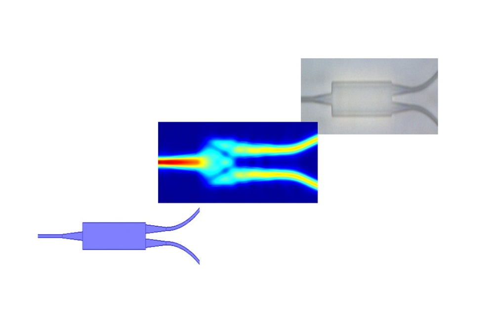
Generate a pool of elementary low-loss plasmonic waveguides on co-planar photonic (Silicon-on-insulator (SOI), SiO2 and Si3N4) substrates based on the CMOS-compatible metals, along with the necessary interfaces to photonic waveguides, by developing the complete technology, fabrication and manufacturability roadmap. Plasmonic as well as hybrid photonic/plasmonic waveguide configurations will be investigated
YEAR 2:
Use PLASMOfab integration platform and components to develop functional PIC prototypes in the μm-scale with superior performance: an optical modulator and a biosensor.
Generate EDA tools for rapid design and prototyping.
Validate PLASMOfab's PIC technology advantages in 2 predominant industrial sectors:
Data communication: Integrate 100 Gb/s SiGe electronics and modulator in a monolithic 100 Gb/s serial NRZ transmitter.
Biosensing: Integrate Si3N4-plasmonic biosensors with microfluidics and high-speed functionalisation techniques in a multichannel, ultra sensitive lab-on-chip for medical diagnostics.
YEAR 3:
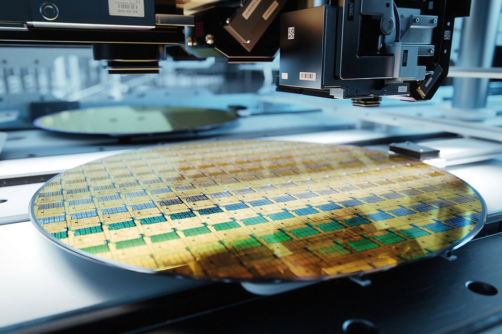
Demonstrate volume manufacturing and cost reduction by complying with large wafer-scale CMOS fabs.
Establish a plasmonics/photonics/electronics fab-less integration service eco-system that may be adopted by commercial silicon and silicon nitride foundry services.
Upon completion PLASMOfab is expected to impact major global markets in photonics unleashing unforeseen capabilities, opportunities and innovations in PIC manufacturing, optical interconnects and networks, opto-electronic transceivers, nano-antennas, medical and environmental sensors as well as magnetic recording and photovoltaics.
The project brings together 5 leading industrial partners and 5 top-ranked academic and research institutes in the PIC and opto-electronics value chain from 6 European countries. PLASMOfab is coordinated by the Aristotle University of Thessaloniki in Greece while the consortium also includes the Université de Bourgogne - member of UBFC (France), the Swiss Federal Institute of Technology in Zurich (Switzerland), AMO GmbH (Germany), ams AG (Austria), Micram Microelectronics GmbH (Germany), Saarland University (Germany), Mellanox (Israel), PhoeniX BV (The Netherlands) and AIT Austrian Institute of Technology GmbH (Austria).
Acknowledgements
PLASMOfab has received funding from the European Union's Horizon 2020 ICT research and innovation program under grant agreement No 688166.


