JePPIX: providing open access to photonic integration
What steps can be taken to streamline the industrialisation of PIC devices and broaden their impact in markets such as metrology, process control and safety systems, as well as supporting new developments in telecoms and data infrastructure? Valentina Moskalenko, Katarzyna Åawniczuk, Meint Smit and Kevin Williams of Europe's JePPIX initiative outline the options that are available through their multi-project wafer programme.
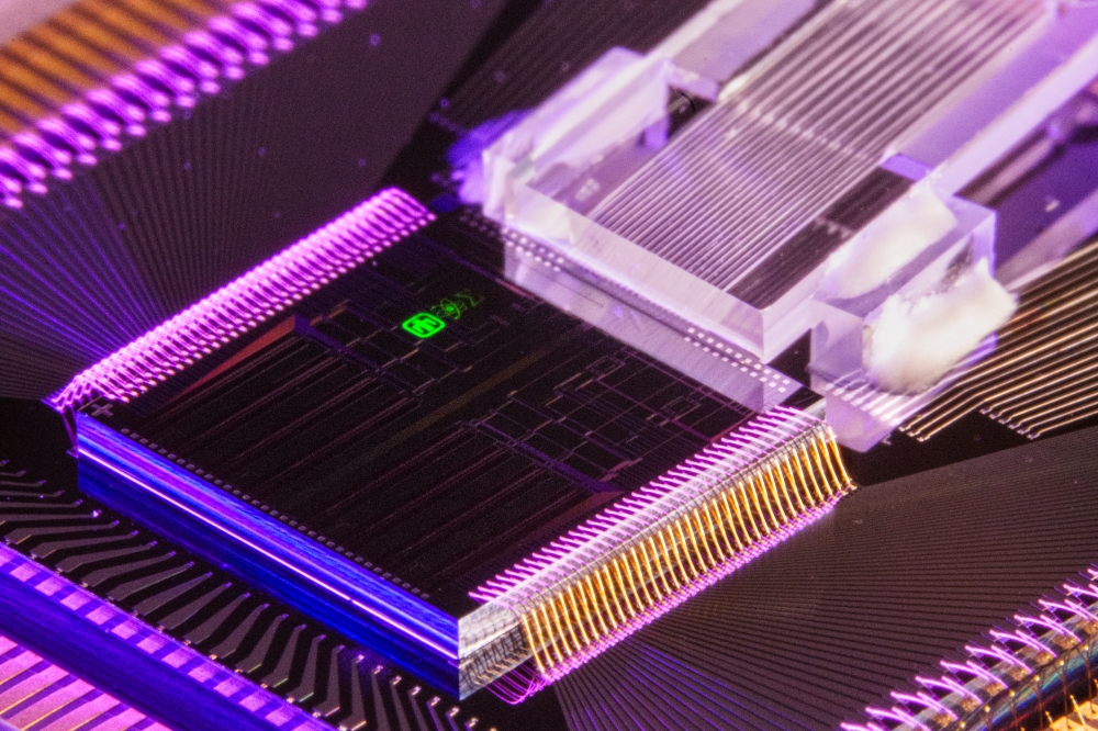
JePPIX is the joint European platform for photonic integration of components and circuits. It is playing a leading role in the industrialisation of generic integration technology by providing open access to InP and Si3N4 integrated photonics. InP integrated photonics is a powerful platform combining laser sources, amplifiers and efficient optoelectronic devices with multiplexers, filters, splitters and interferometers in one chip. Si3N4 TripleX technologies offer low loss circuits with highly complementary material properties. Photonic integrated circuit technology is already established for premium telecommunications solutions and is now poised to revolutionise market segments from metrology and process control through to safety systems and precision imaging. In this article we highlight the powerful process design kits (PDKs), affordable open access using the multi-project wafer (MPW) shuttle runs, and the new opportunities for the PIC community.
Generic integrated photonics
Generic manufacturing enables open access to highly standardised, high performance, photonic integration processes by defining components at the building block level. Complex circuits can then be configured to create new, application-specific PICs without having to know the details of the underlying chip technology. Designers can base their designs on the functional description that is provided in the PDKs. This provides a natural fire-wall between the know-how required for chip production, and the intellectual property associated with product development.
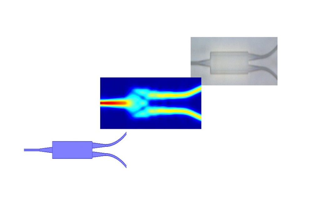
InP integrated photonics offers a particularly powerful platform due to the monolithic integration of light-sources, amplifiers, detectors and modulators with a range of other devices such as interferometers, multiplexers, filters, splitters and mode adaptors. In the MEMPHIS and PARADIGM projects, these components have been implemented as basic building blocks to create the PDK-orientated platforms.
Multi-project shuttle runs
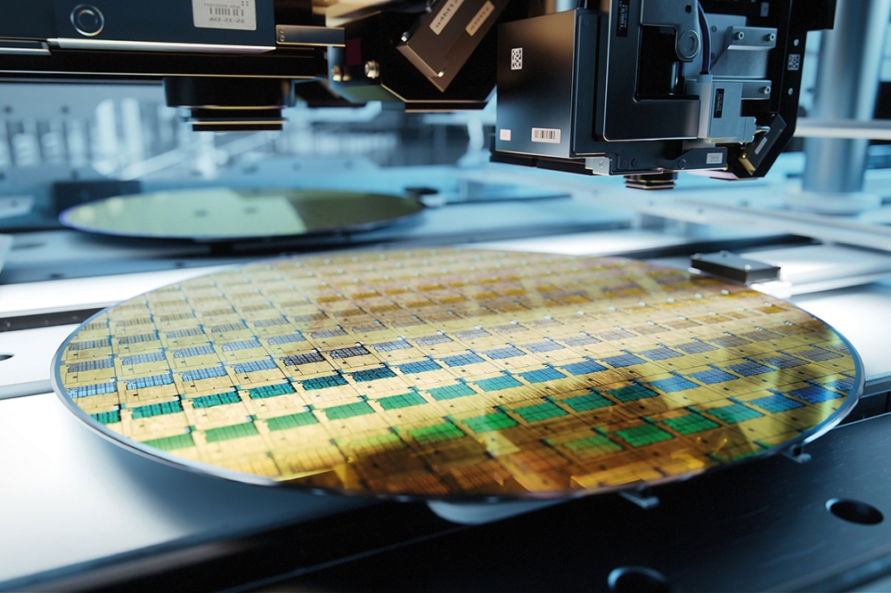
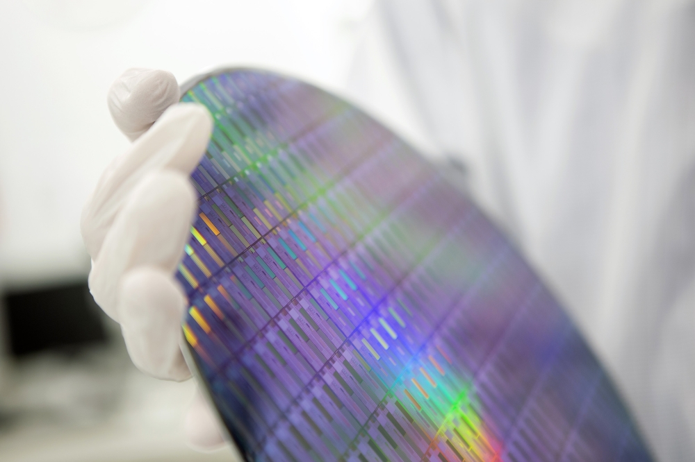
MPW shuttle runs using stable building blocks are the key enablers for affordable PIC prototyping. MPWs can typically support ten independent designs, enabling not only cost sharing on design tools and fab processes, but also at the mask and wafer level. The wafer example in the figure below shows multiple instances of the cells from a number of designers. The gold electrodes indicate a high density of active electro-optic devices. Smart Photonics, Fraunhofer HHI and LioniX all arrange MPW runs with JePPIX.
More news articles


