Addressing the challenges of design automation for photonic integrated circuits
Integrating electronic and photonic design methods is key to unlocking the full potential of PIC devices in the marketplace. Lumerical, Cadence Design Systems and PhoeniX Software review the steps that need to be overcome and propose a pathway towards a unified design automation environment.
Integrating electronic and photonic design methods is key to unlocking the full potential of PIC devices in the marketplace. Lumerical, Cadence Design Systems and PhoeniX Software review the steps that need to be overcome and propose a pathway towards a unified design automation environment.
The design of electronic integrated circuits (EIC) is an established science "“ the industry has decades of experience refining and perfecting its output. Photonic integrated circuit (PIC) design, in contrast, is still in its early stages of development "“ yet to reach the efficient and reliable economies of scale that have been a driving force behind the EIC market. These efficiencies are beginning to emerge in the photonic sector, and as the applications for PIC expand, we are finding that the need to integrate electronic and photonic design methodologies is imperative.
The PIC market is expected to grow to $1.3B (USD) by 2022, expanding at a compound annual growth rate of over 25 percent[1]. Yet, for integrated photonics to become pervasive, design methodologies need to merge into and complement established electronic IC design workflows. Additionally, foundries must take a leading role. Specifically, this means developing robust component libraries and well defined process design kits (PDKs) that application designers can rely on to implement integrated photonics intellectual property and applications. Highly reliable fabrication processes, and component libraries will allow designers to spend more time on system integration and implementation, rather than designing slightly better components.
[1] Transparency Market Research "“ Photonic IC (Hybrid Integration, Monolithic Integration, and Module Integration) Market "“ Global Industry Analysis, Size, Share, Growth, Trends, and Forecast, 2015-2022
Part I: The challenges and the current tools available
There a number of challenges faced by designers that will need to be addressed in order to enable mainstream integrated photonics design and fabrication. Foremost, the tools available to designers must be able to seamlessly and reliably design, test, and optimise both electronic and photonic circuits. This may sound like a straightforward task, but there are significant practical hurdles that make merging the design processes challenging and complex. Integrated photonics design has unique physical and methodological challenges that require specialised tools and methods not used in traditional electronic IC design:
Curvilinear Layout
Component Level Design and Analysis of Photonic Devices
Electronic/Photonic Circuit Simulation
Photonic PDKs
Curvilinear layout
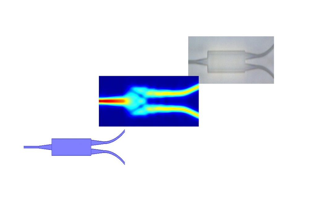
The introduction of curved structures and bends in photonic components and waveguides is potentially the most challenging requirement to address in merging electronic and photonic design methodologies. Unlike the rectilinear (Manhattan-style) routing that is common in electronic IC design, curvilinear features are basic to photonic components. Gradual bends, as opposed to sharp right angles, are critical for retaining light within a waveguide or component.
Figure 1. Three examples of waveguide routing - simulating curved waveguide with different radii. The first image shows a radius of 5 µm; the second 1 µm; and the third .01 µm. Images courtesy Lumerical Solutions.
Small feature geometric effects such as sidewall roughness and discretisation effects introduced from layout parameterised cells (PCells) can have a large impact on the performance characteristics and quality of photonic components and waveguides. Supporting intelligent curved waveguide routing and generation, as well as smooth discretisation of layout PCells become important extensions to traditional rectilinear layout tools.
Component level design and analysis of photonic devices
Active and passive photonic components require unique multi-physics analytical tools to understand and optimise device behavior. Specialised electromagnetic solvers such as mode solvers, eigenmode expansion (EME) or Finite-Difference Time Domain (FDTD) solvers are required to simulate the interaction of light (photons) with matter in nanometer scale geometries; electrical solvers are used to model the behavior of electrons within that same structure. In combination with thermal and process simulators, these sophisticated tools are necessary to optimise device behavior and to extract operating parameters into compact models for simulation at the system level. Compact models for fundamental photonic building blocks like waveguides, splitters, modulators, and photodetectors are necessary for circuit simulation as it is computationally impractical to run full 3D simulation at the circuit level.
Electronic/Photonic Circuit Modelling
There is no widely accepted SPICE equivalent for photonic circuit modelling and optical signal simulation. Since an optical signal is bidirectional and multi-mode, the simulation engine needs to handle amplitude, phase, and ideally model behavior in both frequency and time domains. Complex integrated photonics systems such as a transceivers require simulation of both electrical and photonic sub-circuits. Without an integrated sequential or co-simulation environment where the photonic circuit simulation engine can share data with an electrical circuit simulator, designers are left using multiple simulation tools in separate design environments. Discrete analysis across multiple tools is time consuming, prone to errors, and restrictive for the accurate development of more sophisticated feedback and control systems in transceivers, optical switches or integrated lasers.
Libraries and Fabrication Processes / Process Design Kits
For integrated photonics technology to efficiently leverage the CMOS design ecosystem and impact next generation integrated circuit technology, we require robust, well defined PDKs from validated foundry processes. Most photonic PDKs today are at an early stage, with fixed geometry component libraries and material stackups, limited design rules, and few or no libraries of calibrated compact models for circuit design and optimisation. Photonic components are often optimised through multiple physical design revisions, rather than in simulation prior to fabrication, extending product development times and inflating costs. The pioneering foundries in integrated photonics are beginning to bring more rigorously developed PDKs to market, offering a complete set of design rules, simulation models, and process reliability and variability data. These mature PDKs are the first step towards enabling a fabless design ecosystem for integrated photonics technology where designers can focus on leveraging integrated photonics as a tool to address innovative end applications, rather than as a component level research project.
Part II: Where do we go from here?
The challenges discussed in Part I can be addressed, bringing photonics design into familiar EDA tools and workflows. Focusing on a schematic-driven approach for system design enables designers to create a schematic source for electrical and photonic circuit simulations, as well as layout generation, directly within a single design environment. Standard verification activities such as automated design rule checking (DRC) and layout vs. schematic (LVS) greatly increase the quality and accuracy of designs but also enable automation in waveguide routing and photonic component design.
The market for integrated photonics is poised for expansion. Researchers and leading innovators have identified numerous compelling applications where integrated photonics can potentially revolutionise how we communicate and interact with the physical world. Potent, production-ready design methodologies and tools are critical to enabling a flourishing design ecosystem. Foundries are essential in enabling chip-level designers to leverage photonics as a tool by developing reliable processes, component libraries, and PDKs that allow designers to focus on system level applications for electronic/photonic designs. There are numerous initiatives in Europe and North America that are currently working towards making photonics more accessible "“ IMEC and AIM Photonics are examples that come to mind.
Figure 2. The electronic/photonic design automation (EPDA) Environment developed by Cadence, Lumerical, and PhoeniX Software
Recently Cadence, Lumerical Solutions, and PhoeniX Software partnered to develop an automated flow in order to address the challenges with integrated electronic/photonic design. This new electronic/photonic design automation environment (EPDA) is based on Cadence's Virtuoso® environment, and extended to accommodate photonic design. The seamless integration of PhoeniX Software's advanced algorithms for accurate complex geometry generation and an extensive library of predefined shapes commonly used for photonic components addresses layout challenges. Integrating Lumerical's INTERCONNECT enables the simulation and design of photonic circuits within the Virtuoso environment as well as electro-optical co-simulation with Spectre®. The EPDA flow supports PDK based schematic-driven layout or layout-driven methodologies and together with Lumerical's component-level simulation tools (FDTD Solutions, MODE Solutions, and DEVICE) enables automated PDK development cycles.
As we develop tools and techniques to overcome the challenges of integrated design, such as the EPDA flow described above, PIC designers are creating environments that will help this industry flourish. If photonic designers can continue to rapidly decrease design times, increase productivity and efficiency, we will quickly find ourselves in a space where photonic design is achieving its potential and realising the scale and impact that electronic design has reached over the past few decades.


