University of Utah engineers develop invisibility cloak for high-tech processing chips

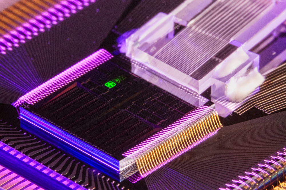
But University of Utah electrical and computer engineering associate professor Rajesh Menon and his team have developed a cloaking device for microscopic photonic integrated devices -- the building blocks of photonic computer chips that run on light instead of electrical current -- in an effort to make future chips smaller, faster and consume much less power.
Menon's discovery was published online Wednesday in the latest edition of the science journal, Nature Communications. The paper was co-written by University of Utah doctoral student Bing Shen and Randy Polson, senior optical engineer in the University of Utah's Nanofab.
The future of computers, data centres and mobile devices will involve photonic chips in which data is shuttled around and processed as light photons instead of electrons. The advantages of photonic chips over today's silicon-based chips are they will be much faster and consume less power and therefore give off less heat. And inside each chip are potentially billions of photonic devices, each with a specific function in much the same way that billions of transistors have different functions inside today's silicon chips. For example, one group of devices would perform calculations, another would perform certain processing, and so on.
The problem, however, is if two of these photonic devices are too close to each other, they will not work because the light leakage between them will cause "crosstalk" much like radio interference. If they are spaced far apart to solve this problem, you end up with a chip that is much too large.
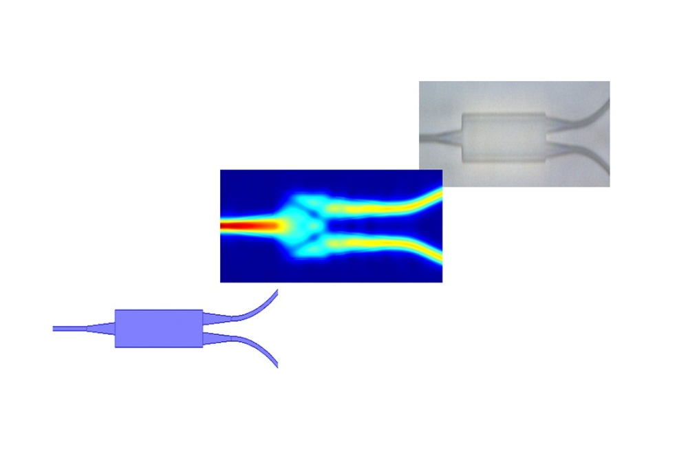
So Menon and his team discovered you can put a special nanopatterened silicon-based barrier in between two of the photonic devices, which acts like a "cloak" and tricks one device from not seeing the other.
"The principle we are using is similar to that of the Harry Potter invisibility cloak," Menon says. "Any light that comes to one device is redirected back as if to mimic the situation of not having a neighbouring device. It's like a barrier -- it pushes the light back into the original device. It is being fooled into thinking there is nothing on the other side."
Consequently, billions of these photonic devices can be packed into a single chip, and a chip can contain more of these devices for even more functionality. And since these photonic chips use light photons instead of electrons to transfer data, which builds up heat, these chips potentially could consume 10 to 100 times less power, which would be a boon for places like data centres that use tremendous amounts of electricity.
Menon believes the most immediate application for this technology and for photonic chips in general will be for data centres similar to the ones used by services like Google and Facebook. According to a study from the U.S. Department of Energy's Lawrence Berkeley National Laboratory, data centres just in the U.S. consumed 70 billion kWh in 2014, or about 1.8 percent of total U.S. electricity consumption. And that power usage is expected to rise another 4 percent by 2020.


